
Last Updated May 28, 2026
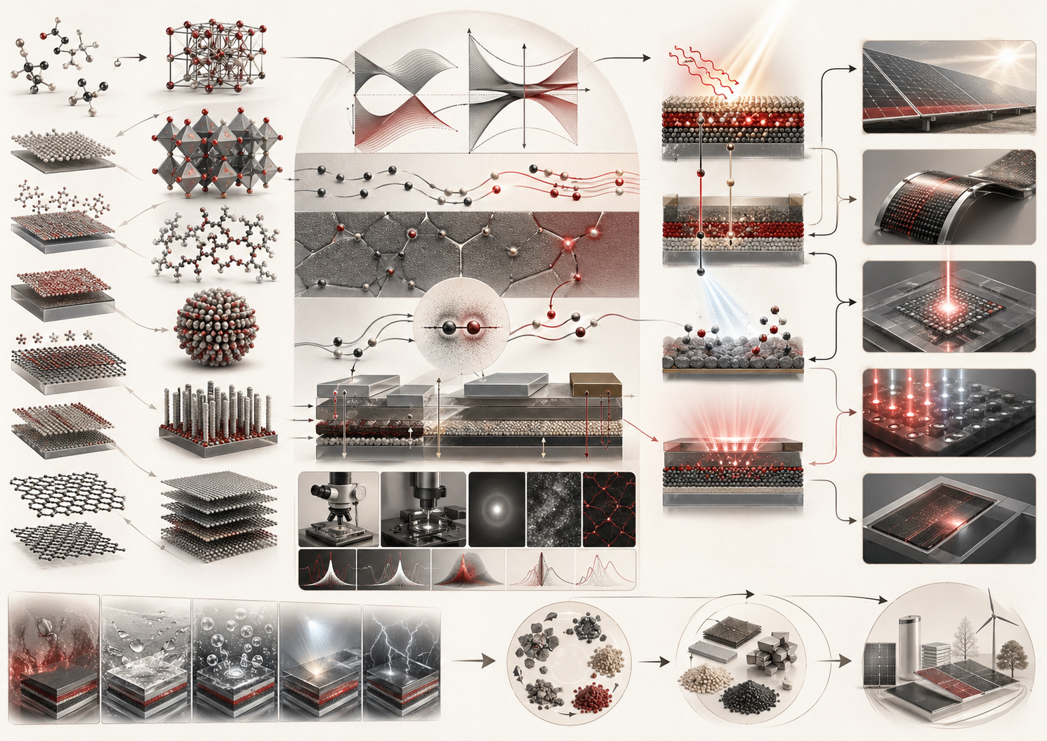
Semiconductor, electronic, and photochemical materials connect chemistry to charge, light, information, sensing, energy conversion, and molecular transformation. They include silicon, compound semiconductors, metal oxides, organic semiconductors, perovskites, quantum dots, conjugated polymers, photoactive dyes, photocatalysts, phosphors, dielectrics, electrodes, thin films, two-dimensional materials, nanowires, molecular electronics, and hybrid organic-inorganic systems. These materials are chemically important because their function depends on electronic structure, defects, interfaces, excited states, transport, stability, processing, and interaction with light.
The central thesis of this article is that electronic and photoactive materials cannot be understood from composition alone. Their behavior depends on band structure, bonding, crystal quality, morphology, dopants, traps, grain boundaries, charge-carrier mobility, recombination, surface chemistry, device architecture, illumination, degradation, and measurement conditions. A semiconductor is not merely a formula. A photovoltaic absorber is not merely a band gap. A photocatalyst is not merely a material that absorbs light. Function emerges from the coupling of chemical structure, electronic states, interfaces, and operating environment.
These materials are therefore a bridge between molecular chemistry and technological systems. They connect electrons and photons to computing, sensing, lighting, photovoltaics, catalysis, communications, analytical instruments, environmental monitoring, and infrastructure. To understand them chemically is to understand how matter can be designed to move charge, absorb light, emit light, separate carriers, store information, detect chemical signals, and drive reactions under controlled conditions.
Main Library
Publications
Article Map
Chemistry
Related Topic
Physics
Related Topic
Embedded & Edge Systems
Related Topic
Data Systems & Analytics
Why Electronic and Photochemical Materials Matter
Electronic and photochemical materials are among the most consequential materials in modern chemistry because they mediate the movement of charge and the absorption, emission, or conversion of light. They make possible integrated circuits, solar cells, LEDs, lasers, displays, sensors, detectors, photocatalysts, memory devices, batteries, transistors, electrochromic coatings, photochemical reactors, and many analytical instruments.
The chemical challenge is not simply to identify materials that contain useful elements. The challenge is to design matter so that electrons, holes, excitons, ions, photons, defects, and interfaces behave in controlled ways. A semiconductor must have an appropriate band gap. A photovoltaic absorber must absorb light, create charge carriers, separate them, transport them, and resist degradation. A photocatalyst must absorb photons and drive chemical transformations before excited states recombine. A dielectric must insulate under electric field. A sensor material must respond selectively and reproducibly. An organic electronic material must transport charge while surviving oxygen, water, light, heat, and mechanical stress.
These materials therefore sit at the intersection of physical chemistry, materials chemistry, solid-state chemistry, surface chemistry, photochemistry, electrochemistry, spectroscopy, device physics, and sustainable technology. They require chemical knowledge of bonding, defects, oxidation states, coordination environments, molecular orbitals, lattice structure, morphology, surface termination, and interfacial reactivity. They also require engineering awareness of processing, device architecture, testing standards, reliability, scale-up, and end-of-life recovery.
Their importance is not only technological. Electronic and photochemical materials shape public infrastructure. Solar absorbers affect renewable-electricity generation. Power electronics affect electrification efficiency. Sensors affect environmental monitoring, medicine, manufacturing, and safety. LEDs affect lighting energy demand. Photocatalysts may affect chemical synthesis, water treatment, or pollutant transformation. Semiconductors underpin computing, communications, data systems, embedded devices, and automation.
For researchers and scientists, the key lesson is that function depends on structure across scales. Atomic composition matters, but so do crystal quality, phase purity, grain boundaries, dopants, defects, interfaces, film processing, device geometry, operating conditions, and degradation pathways. The material cannot be separated from how it is made, measured, and used.
Semiconductors and Band Structure
A semiconductor is a material whose electrical conductivity can be controlled by composition, defects, dopants, temperature, light, electric field, and interfaces. Semiconductors differ from metals and insulators because their electronic band structure creates a tunable gap between occupied and unoccupied electronic states. Electrons can be promoted across this gap thermally, optically, chemically, or electrically.
The band gap is one of the central concepts in semiconductor chemistry. A small band gap can permit absorption of lower-energy light and greater intrinsic conductivity. A large band gap can make a material transparent or insulating under ordinary conditions. The band gap affects color, conductivity, photovoltaic behavior, photodetection, photocatalysis, and light emission.
Semiconductors may be elemental, compound, organic, hybrid, crystalline, amorphous, nanostructured, two-dimensional, or molecularly engineered. Important examples include:
- silicon and germanium;
- compound semiconductors such as gallium arsenide, gallium nitride, indium phosphide, cadmium telluride, and copper indium gallium selenide;
- metal oxides such as titanium dioxide, zinc oxide, tin oxide, nickel oxide, and indium tin oxide;
- hybrid perovskites and related halide materials;
- organic semiconductors and conjugated polymers;
- quantum dots and semiconductor nanocrystals;
- two-dimensional semiconductors such as transition-metal dichalcogenides.
Band structure is not determined by chemical formula alone. It depends on bonding, crystal structure, strain, dimensionality, defects, surface termination, quantum confinement, doping, disorder, and phase purity. Two samples with the same nominal composition can have different electronic behavior if one is crystalline and the other amorphous, if one contains deep traps and the other does not, or if one has different grain boundaries, impurities, or surface states.
Doping is especially important. Intentional dopants introduce electronic states that increase electron or hole concentration. In silicon, controlled doping makes p-type and n-type materials, enabling diodes, transistors, and integrated circuits. In metal oxides, oxygen vacancies or aliovalent dopants can change conductivity. In organic semiconductors, molecular dopants can change carrier density but may also affect morphology and stability. Doping is therefore chemical control of electronic population.
For researchers, semiconductor chemistry requires distinguishing ideal band diagrams from real materials. Real semiconductors contain defects, surfaces, interfaces, strain, impurities, and finite-size effects. These features may be useful, harmful, or both depending on application. A defect that improves catalytic activity may harm photovoltaic performance by increasing recombination. A grain boundary that is tolerable in one device may be catastrophic in another. Semiconductor chemistry is the science of useful imperfection as much as ideal structure.
Electronic Materials, Charge Transport, and Devices
Electronic materials are designed to control charge movement, charge storage, insulation, switching, conduction, polarization, sensing, or emission. They include conductors, semiconductors, insulators, dielectrics, ferroelectrics, piezoelectrics, thermoelectrics, ionic conductors, transparent conducting oxides, magnetic materials, and mixed ionic-electronic conductors.
Charge transport depends on carrier concentration, carrier mobility, scattering, traps, defects, interfaces, morphology, temperature, and electric field. In crystalline inorganic semiconductors, transport may be dominated by band-like conduction and scattering. In organic semiconductors, transport may involve hopping, disorder, molecular packing, energetic traps, and grain boundaries. In mixed conductors, both ions and electrons may move. In nanomaterials, surfaces and interfaces may dominate behavior.
Electronic devices translate material properties into function. A transistor requires controlled charge injection, channel transport, gate modulation, contacts, dielectric stability, and low leakage. A photodiode requires light absorption, carrier separation, and low noise. A light-emitting diode requires carrier injection, recombination, emission, and optical extraction. A memory material requires stable, switchable states. A sensor requires selective response, reversibility, calibration, and drift control.
This is why electronic-materials chemistry must be linked to device architecture. A material with promising intrinsic properties can fail if contacts are poor, surfaces are unstable, films are rough, grain boundaries trap carriers, interfaces recombine charges, or processing damages the active layer. A high-mobility material may be useless in a device if it cannot form stable films or low-resistance contacts. A dielectric may have excellent insulating properties in bulk but fail at interfaces under high field or humidity.
Electronic materials also require stability under bias. Electric fields can move ions, induce defects, shift thresholds, create trapped charge, accelerate corrosion, or promote breakdown. Bias stress is especially important in thin-film transistors, perovskite devices, oxide electronics, organic electronics, and memory materials. Device operation is therefore a chemical stress test.
For researchers, the material-device relationship should be treated as part of the evidence. Reporting only intrinsic material properties can be misleading if the application depends on contacts, interfaces, geometry, encapsulation, and operation. A material becomes electronic only through a working architecture.
Photochemical Materials and Excited States
Photochemical materials absorb light and form excited states. An excited state is a state of a system with energy higher than its ground state. In photochemical systems, absorption of a photon can promote an electron to a higher-energy state, creating an electronically excited molecule, exciton, charge-transfer state, electron-hole pair, or surface-trapped carrier.
Excited states are chemically powerful because they can emit light, transfer energy, transfer electrons, undergo bond cleavage, initiate polymerization, sensitize reactions, isomerize, generate radicals, form triplet states, or drive redox chemistry. They are also fragile because they may deactivate through fluorescence, phosphorescence, internal conversion, intersystem crossing, vibrational relaxation, quenching, recombination, or nonradiative decay.
Photochemical materials include:
- photoactive dyes and sensitizers;
- photoinitiators for polymerization;
- photochromic and photoswitchable molecules;
- photocatalysts and photosensitizers;
- fluorescent probes and phosphors;
- semiconductor absorbers;
- quantum dots and nanocrystals;
- organic light-emitting materials;
- photoredox catalysts;
- light-responsive polymers and surfaces.
Photochemical design requires matching absorption spectrum, excited-state lifetime, redox potential, intersystem crossing, energy transfer, solubility, stability, and reaction environment. A molecule that absorbs strongly may still be a poor photochemical material if it deactivates too quickly, decomposes under illumination, aggregates, quenches itself, or cannot transfer charge or energy to the desired substrate.
Excited-state pathways are highly sensitive to environment. Solvent polarity can shift emission, stabilize charge-transfer states, or alter photoredox behavior. Oxygen can quench triplet states or generate reactive oxygen species. Aggregation can either quench luminescence or enhance emission depending on material class. Surfaces can trap carriers or support charge separation. Photochemistry is therefore inseparable from local chemical context.
For researchers, photochemical materials require careful controls. Light intensity, wavelength, optical path length, photon flux, concentration, oxygen, solvent, temperature, sample thickness, scattering, and degradation all affect results. Photochemical claims become weak when illumination and product measurement are not specified.
Photovoltaic and Solar-Energy Materials
Photovoltaic materials convert light into electrical energy. The basic sequence is light absorption, excited-state or electron-hole pair formation, charge separation, charge transport, charge collection, and external power generation. Each step can be limited by recombination, defects, interface barriers, poor mobility, instability, parasitic absorption, poor contacts, or degradation.
Silicon remains the dominant photovoltaic material because it combines abundance, strong processing infrastructure, long-term stability, and mature device engineering. Thin-film technologies such as cadmium telluride and copper indium gallium selenide offer different processing and absorption advantages. Organic photovoltaics provide flexibility and tunable chemistry. Perovskite photovoltaics have attracted major attention because they can combine strong absorption, promising charge-transport behavior, and solution or vapor processing, while still requiring careful work on stability, interfaces, environmental compatibility, and scalable manufacturing.
Solar-energy materials include more than absorbers. They require transparent conductors, charge-transport layers, passivation layers, encapsulants, contacts, substrates, adhesives, barrier films, and protective coatings. The chemistry of interfaces often determines whether a solar device performs well and survives outdoors.
Photovoltaic performance metrics include short-circuit current density, open-circuit voltage, fill factor, power conversion efficiency, external quantum efficiency, spectral response, series resistance, shunt resistance, hysteresis, temperature coefficient, degradation rate, and lifetime. These metrics must be reported under defined illumination, temperature, active area, scan direction, calibration, stabilization protocol, and device history.
Photovoltaics also demonstrate the difference between laboratory efficiency and deployment value. A high-efficiency laboratory cell may rely on small area, expensive substrates, unstable interfaces, toxic precursors, non-scalable processing, or short-duration testing. A slightly lower-efficiency technology may be more valuable if it is durable, manufacturable, repairable, abundant, recyclable, and safe. Solar-materials chemistry must therefore connect performance with reliability and lifecycle design.
For researchers, photovoltaic materials are not simply energy materials. They are optoelectronic systems whose value depends on photon absorption, carrier lifetime, selective contacts, interfacial passivation, film morphology, encapsulation, and outdoor degradation behavior.
Photocatalysis and Light-Driven Chemical Transformation
Photocatalysis uses light-absorbing materials to accelerate chemical transformations. A photocatalyst absorbs photons, forms excited carriers or excited states, and transfers energy or charge to reactants. Photocatalysis can support water splitting, carbon dioxide reduction, pollutant degradation, organic synthesis, nitrogen transformation, hydrogen production, oxygen evolution, and antimicrobial surfaces.
In semiconductor photocatalysis, photon absorption generates electron-hole pairs. These carriers must reach reactive sites before recombining. Surface reactions may require adsorbed water, oxygen, carbon dioxide, protons, substrates, sacrificial donors, or co-catalysts. The surface chemistry of a photocatalyst is therefore just as important as its optical absorption.
Photocatalytic activity depends on band alignment, absorption spectrum, carrier lifetime, diffusion length, surface area, crystallinity, defects, co-catalyst loading, reactant adsorption, pH, solvent, oxygen, sacrificial agents, product desorption, and illumination conditions. A material with a suitable band gap may still fail if its carriers recombine too quickly or if its surface cannot catalyze the required half-reactions.
Photocatalytic claims require caution. A material may degrade a dye under illumination but fail in real water matrices. A catalyst may produce hydrogen in the presence of sacrificial reagents but not split water overall. A carbon dioxide reduction system may produce trace products that require rigorous controls. Responsible photocatalysis requires product identification, quantum-yield or efficiency estimates, dark controls, light controls, catalyst stability testing, mass balance, isotope controls where appropriate, and realistic conditions.
Photocatalysis is especially vulnerable to overinterpretation because apparent activity can arise from adsorption, photolysis, dye sensitization, contamination, sacrificial reagents, leaching, or analytical artifacts. A strong photocatalysis study distinguishes true catalytic transformation from disappearance of a visible signal. It measures products, not just color loss.
For researchers, photocatalysis is most powerful when it is treated as interfacial photochemistry under mass-balance discipline. Light absorption starts the process, but surface chemistry, transport, selectivity, stability, and measurement quality determine whether useful transformation occurs.
Organic, Hybrid, and Molecular Electronic Materials
Organic and hybrid electronic materials extend electronic function beyond traditional crystalline inorganic solids. Conjugated molecules and polymers can transport charge, absorb light, emit light, change color, switch states, or respond to chemical environments. Hybrid materials combine organic and inorganic components to tune processing, flexibility, interfaces, dielectric behavior, optical absorption, and charge transport.
Organic semiconductors are important in OLEDs, organic photovoltaics, field-effect transistors, sensors, bioelectronics, and flexible electronics. Their function depends on molecular orbital energies, conjugation length, packing, crystallinity, disorder, morphology, phase separation, dopants, contacts, and environmental stability. A polymer with excellent electronic structure may perform poorly if it forms disordered films, traps charges, or phase-separates unpredictably.
Molecular electronics and photochemical materials also show how chemical structure can be translated into electronic function. Donor-acceptor molecules can support charge transfer. Photochromic molecules can switch under light. Redox-active molecules can store charge. Metal complexes can harvest light, transfer electrons, or emit. Porphyrins, phthalocyanines, ruthenium complexes, iridium complexes, organic dyes, and photoredox catalysts are all examples of chemistry designed around electronic and excited-state behavior.
Hybrid perovskites illustrate both the promise and difficulty of hybrid materials. They can show strong absorption, long carrier diffusion lengths, and tunable composition, but they can also be sensitive to moisture, oxygen, heat, light, bias, ion migration, and interfacial degradation. Their performance depends not only on formula but on film formation, grain boundaries, passivation, transport layers, encapsulation, and device architecture.
Organic and hybrid materials also emphasize processing as chemistry. Solvent choice, drying rate, annealing, additives, humidity, substrate energy, crystallization pathway, and film thickness can change morphology and performance. A material may not have one intrinsic device behavior; it may have many behaviors depending on how it is processed.
For researchers, organic and hybrid materials require connecting molecular design to mesoscale structure. The molecule matters, but so does the film. Electronic function emerges from chemical structure organized into material architecture.
Quantum Dots, Nanowires, and Two-Dimensional Materials
Nanostructured electronic and photochemical materials can behave differently from bulk materials because size, surface area, confinement, and dimensionality change electronic and optical properties. Quantum dots, semiconductor nanocrystals, nanowires, nanosheets, transition-metal dichalcogenides, graphene-related systems, and other low-dimensional structures allow chemists to tune function through size, shape, surface ligands, defects, and assembly.
Quantum dots can show size-dependent absorption and emission because quantum confinement changes energy levels. Smaller particles often have larger effective band gaps than larger particles of the same material. This makes nanocrystals useful for displays, bioimaging, photodetectors, LEDs, and solar-energy concepts. Their behavior depends on core composition, shell structure, surface ligands, trap states, size distribution, and environmental stability.
Nanowires can provide directional charge transport, high surface area, and strain relaxation. They are studied for sensors, photodetectors, energy harvesting, electronics, and catalysis. Two-dimensional semiconductors can show thickness-dependent band structures, strong excitonic effects, surface sensitivity, and interface-dominated transport. Their properties depend on layer number, defects, substrate, strain, edge chemistry, contacts, and contamination.
Nanomaterials also raise measurement and responsibility questions. High surface area can improve activity but increase reactivity and instability. Ligands can stabilize particles but impede charge transport. Quantum dots may contain toxic elements. Nanoparticles can be difficult to recover if released. A nanoscale material may perform well in a device but create manufacturing, exposure, or end-of-life concerns. Useful nanoscale design requires both performance and containment thinking.
For researchers, nanostructured materials demonstrate that electronic function can be chemically tuned beyond composition. Size, surface, and dimensionality become design variables. But they also make reproducibility harder because small changes in synthesis, purification, ligand exchange, or assembly can change properties substantially.
Defects, Interfaces, and Degradation
Defects are central to semiconductor, electronic, and photochemical materials. Some defects are useful. Dopants intentionally introduce carriers. Oxygen vacancies can influence conductivity and catalysis. Controlled impurities can tune electronic behavior. But uncontrolled defects can trap carriers, accelerate recombination, create leakage pathways, shift thresholds, quench luminescence, or initiate degradation.
Interfaces are equally important. Semiconductor devices are built from interfaces: absorber-contact, semiconductor-dielectric, grain boundary, electrode-electrolyte, donor-acceptor, organic-inorganic, oxide-metal, perovskite-transport layer, quantum dot-ligand, and film-substrate interfaces. These boundaries can separate charge, block recombination, align energy levels, stabilize surfaces, or create failure pathways.
Degradation can occur through oxidation, hydrolysis, photobleaching, ion migration, interdiffusion, delamination, crystallization, amorphization, phase segregation, electrode reaction, thermal stress, ultraviolet exposure, moisture, oxygen, bias stress, and mechanical fatigue. Electronic and photochemical materials must therefore be evaluated not only for initial performance but for performance over time under realistic operating conditions.
Defects and interfaces often control lifetime more strongly than bulk composition. A small concentration of deep traps can reduce carrier lifetime. A poorly passivated surface can dominate recombination. A contact that reacts slowly with the active layer can destroy a device under bias. Moisture entering through imperfect encapsulation can initiate degradation even when the active material appears stable in dry laboratory conditions.
Degradation also affects interpretation. If performance improves during early operation, it may reflect activation, ion migration, trap filling, contact adjustment, or measurement artifact. If performance decays, it may reflect chemical decomposition, interfacial change, phase segregation, contact failure, film cracking, or optical changes. Time-dependent data are therefore essential.
For researchers, defect and interface control is not secondary. It is often the difference between a promising material and a useful technology. A material’s future is frequently determined at its boundaries.
Processing, Thin Films, and Manufacturing Sensitivity
Electronic and photochemical materials often function as thin films, patterned layers, nanostructures, coated surfaces, printed devices, vapor-deposited stacks, or solution-processed architectures. Processing determines morphology, defect density, crystallinity, grain size, orientation, phase purity, surface roughness, residual solvent, contamination, and interface quality. A material’s chemistry cannot be separated from how it is made.
Common processing methods include chemical vapor deposition, physical vapor deposition, sputtering, atomic layer deposition, spin coating, slot-die coating, blade coating, inkjet printing, spray coating, electrodeposition, sol-gel processing, thermal evaporation, epitaxy, annealing, photolithography, etching, ligand exchange, and self-assembly. Each method introduces constraints and opportunities. A high-temperature method may produce high-quality films but limit substrates. A low-temperature solution method may enable flexible devices but introduce solvent, drying, and morphology challenges.
Thin-film processing is especially sensitive because small variations can alter performance. Humidity can change perovskite crystallization. Solvent evaporation can change polymer morphology. Annealing can improve ordering or cause phase segregation. Substrate cleanliness can affect nucleation. Residual ions can cause drift. Film thickness can change absorption and transport. Surface roughness can create shunts or contact problems.
Manufacturing sensitivity matters for translation. A material that works in a small laboratory device may be difficult to scale to large-area films with uniform thickness, low defect density, stable interfaces, and high yield. A device that performs on a rigid glass substrate may not perform on flexible plastic. A process that uses rare solvents, glovebox conditions, or slow annealing may be difficult to deploy responsibly.
For researchers, processing conditions should be treated as part of the material record. A reported performance value without processing history is incomplete. In electronic and photochemical materials, synthesis and processing are not preparation details; they are functional variables.
Characterization and Measurement
Electronic and photochemical materials require characterization across structure, composition, electronic properties, optical response, morphology, surfaces, interfaces, and stability. No single method is sufficient. A material may have an attractive absorption spectrum but poor charge transport. It may have high mobility in a single crystal but poor performance in a thin film. It may have strong photoluminescence but poor device stability. It may show impressive activity in one test but fail under realistic illumination or environmental exposure.
Common characterization methods include:
- UV-visible absorption spectroscopy;
- photoluminescence and time-resolved photoluminescence;
- Raman and infrared spectroscopy;
- X-ray diffraction and grazing-incidence diffraction;
- electron microscopy and atomic force microscopy;
- X-ray photoelectron spectroscopy and ultraviolet photoelectron spectroscopy;
- electrical conductivity and Hall measurements;
- current-voltage and capacitance-voltage testing;
- impedance spectroscopy;
- transient absorption spectroscopy;
- external quantum efficiency measurement;
- stability, thermal cycling, humidity, light-soaking, and bias-stress tests.
Measurement must match the claim. A semiconductor band gap estimated from optical absorption is not necessarily the same as an electronic transport gap. A device efficiency requires defined illumination, area, calibration, hysteresis control, and stability conditions. A photocatalytic yield requires product quantification and appropriate controls. A photoluminescent quantum yield requires calibrated optical measurement. A material described as stable requires time-dependent evidence under relevant stressors.
Device measurements require special caution. Current-voltage curves can be distorted by scan rate, hysteresis, series resistance, shunts, capacitance, temperature, light soaking, and unstable interfaces. Reported efficiency can be inflated by incorrect active-area definition, poor calibration, transient behavior, or failure to stabilize output. Photocatalytic metrics can be distorted by adsorption, incomplete product detection, or uncontrolled light flux. Sensor metrics can be distorted by drift, matrix effects, fouling, and calibration instability.
For researchers, the strongest characterization programs combine structural, optical, electrical, chemical, surface, and stability evidence. One measurement can suggest a mechanism; converging measurements can support one.
From Material Property to Device Performance
A material property is not the same as device performance. A high carrier mobility in a single crystal does not guarantee high current in a thin-film transistor. A strong absorption coefficient does not guarantee high solar-cell efficiency. A long photoluminescence lifetime does not automatically mean efficient charge collection. A high catalytic activity in a small test does not guarantee durable operation under realistic flows, impurities, or illumination.
Device translation requires matching material function to architecture. Contacts must inject or extract charge. Interfaces must align energy levels. Layers must be physically continuous and chemically compatible. The device must manage heat, light, moisture, oxygen, mechanical stress, and electrical bias. Packaging and encapsulation must protect the active material without blocking function. Measurement must distinguish intrinsic material limits from device-design problems.
This translation problem explains why interdisciplinary work is essential. Chemists can design molecular structures, surfaces, and synthesis routes. Materials scientists can control morphology and phase. Physicists can model charge transport and optical behavior. Engineers can design devices and manufacturing processes. Data scientists can analyze high-dimensional measurements and stability trends. Responsible deployment requires all of these perspectives.
Device translation also requires lifetime thinking. A material that performs well initially may fail through slow degradation. A device that survives dry nitrogen may fail outdoors. A sensor that works in clean buffer may fail in wastewater, blood, soil, or air with interfering compounds. A photocatalyst that works with purified reactants may foul in real matrices. Performance must be tested in the environment implied by the claim.
For researchers, the practical rule is simple: do not let a promising material property stand in for a working system. The system must be built, measured, stressed, aged, and interpreted with the same rigor as the material itself.
Sustainability, Critical Materials, and Responsible Design
Semiconductor, electronic, and photochemical materials are central to sustainable technology, but they are not automatically sustainable. Solar cells, LEDs, sensors, power electronics, batteries, and photocatalysts can support energy transition, efficiency, monitoring, and cleaner chemical processes. Yet they may also involve critical elements, toxic precursors, energy-intensive processing, hazardous solvents, difficult recycling, electronic waste, fluorinated materials, rare metals, and stability challenges.
Responsible design requires evaluating both function and consequence. A high-performance material may depend on scarce elements. A low-temperature process may use problematic solvents. A photocatalyst may degrade pollutants in the laboratory but release transformation products or particles into the environment. A photovoltaic material may convert sunlight efficiently but require encapsulation, recovery, and end-of-life planning. An electronic material may function well but be difficult to separate from multilayer devices.
Important responsible-design questions include:
- Does the material depend on scarce, toxic, conflict-associated, geopolitically concentrated, or difficult-to-recover elements?
- Can processing temperature, solvent burden, water use, and waste be reduced?
- Does the material remain stable under light, heat, oxygen, moisture, and bias?
- Are degradation products known and acceptable?
- Can the device or material be repaired, recovered, recycled, or safely contained?
- Does the material improve energy or chemical performance enough to justify its lifecycle impacts?
- Are performance claims based on realistic operating conditions?
- Does deployment shift exposure or waste burdens onto workers, communities, or downstream processors?
Responsible design also requires avoiding substitution traps. A replacement material may remove one concern while introducing another: lower toxicity but poorer durability, lower temperature but higher solvent burden, higher efficiency but harder recycling, reduced critical-metal dependence but greater instability. Sustainable materials design requires a full accounting of performance, stability, manufacturing, exposure, recovery, and system context.
The ethical strength of electronic and photochemical materials chemistry lies in linking molecular and solid-state function to transparent measurement, durability, lifecycle thinking, and responsible deployment. These materials can support more efficient and less carbon-intensive systems, but only if their own material flows and risks are taken seriously.
Mathematical Lens: Band Gaps, Photons, Transport, and Quantum Yield
The energy of a photon is:
E = h\nu = \frac{hc}{\lambda}
\]
Interpretation: \(E\) is photon energy, \(h\) is Planck’s constant, \(\nu\) is frequency, \(c\) is the speed of light, and \(\lambda\) is wavelength. This relationship connects light color to energy.
A simplified semiconductor absorption threshold can be related to the band gap:
E_g \approx \frac{1240}{\lambda_{\mathrm{edge}}}
\]
Interpretation: \(E_g\) is band-gap energy in electronvolts and \(\lambda_{\mathrm{edge}}\) is absorption edge in nanometers. This approximation is useful for intuition, but real band-gap estimation requires attention to direct versus indirect transitions, excitons, disorder, scattering, thickness, and method.
Electrical conductivity can be represented as:
\sigma = q(n\mu_n + p\mu_p)
\]
Interpretation: \(\sigma\) is conductivity, \(q\) is elementary charge, \(n\) and \(p\) are electron and hole concentrations, and \(\mu_n\) and \(\mu_p\) are electron and hole mobilities. Conductivity depends on both how many carriers exist and how easily they move.
Carrier diffusion length is often approximated as:
L = \sqrt{D\tau}
\]
Interpretation: \(L\) is diffusion length, \(D\) is diffusion coefficient, and \(\tau\) is carrier lifetime. Longer diffusion lengths can improve charge collection when carriers must travel through a material before recombining.
Photochemical quantum yield is commonly expressed as:
\Phi = \frac{\mathrm{number\ of\ events}}{\mathrm{number\ of\ photons\ absorbed}}
\]
Interpretation: The event may be product molecules formed, photons emitted, molecules reacted, or charge carriers collected, depending on context. Quantum yield makes photochemical efficiency explicit, but it must be measured under well-defined optical and chemical conditions.
External quantum efficiency in a photovoltaic or photodetector context can be written as:
EQE = \frac{\mathrm{collected\ charge\ carriers}}{\mathrm{incident\ photons}}
\]
Interpretation: \(EQE\) connects optical input to electrical output. It includes absorption, charge separation, transport, and collection losses.
A simplified photovoltaic fill factor is:
FF = \frac{P_{\mathrm{max}}}{J_{SC}V_{OC}}
\]
Interpretation: \(P_{\mathrm{max}}\) is maximum power density, \(J_{SC}\) is short-circuit current density, and \(V_{OC}\) is open-circuit voltage. Fill factor reflects series resistance, shunts, recombination, transport, and device quality.
Power conversion efficiency can be expressed as:
\eta = \frac{J_{SC}V_{OC}FF}{P_{\mathrm{in}}}
\]
Interpretation: \(P_{\mathrm{in}}\) is incident optical power density. Efficiency claims require calibrated illumination, defined active area, stable output, and controlled measurement conditions.
These equations clarify the structure of light- and charge-based materials. Photon energy determines possible excitation. Band gap influences absorption and electronic transitions. Mobility and carrier concentration determine conductivity. Lifetime and diffusion determine carrier survival. Quantum yield and efficiency connect microscopic events to measurable function.
Computational Workflows for Electronic and Photochemical Materials
Computational workflows can make materials comparison more transparent. A workflow can track material class, composition, band gap, mobility, carrier lifetime, absorption edge, photostability, processing temperature, critical-material flags, device metrics, stability decay, measurement method, uncertainty, and responsible-design review status. This is useful because electronic and photochemical performance depends on many coupled variables.
Useful workflows include band-gap screening, mobility comparison, photostability ranking, quantum-yield analysis, device-replicate summaries, photovoltaic efficiency calculation, photocatalytic product normalization, degradation-slope estimation, processing-temperature comparison, critical-material flagging, and data-provenance tracking. More advanced workflows may integrate high-throughput computation, experimental synthesis databases, spectroscopy files, microscopy metadata, device-test histories, machine-learning models, and lifecycle assessment.
For researchers, computational workflows should preserve measurement context. A band gap from density-functional theory is not identical to an optical absorption edge. Mobility from a single crystal is not identical to mobility in a processed thin film. A device efficiency measured under one illumination protocol may not be comparable to another. A stability score without stress conditions is weak. A ranking model is useful only when its assumptions are visible.
The examples below use synthetic data. They do not qualify materials, certify devices, predict real lifetime, establish product claims, validate photovoltaic performance, or replace professional materials characterization. They demonstrate how electronic and photochemical materials reasoning can be structured, audited, and communicated responsibly.
Python Example: Screening Electronic and Photochemical Materials
The following Python example uses synthetic educational data to screen candidate electronic and photochemical materials. It combines band gap, mobility, lifetime, absorption edge, photostability, critical-material concerns, and processing temperature into a transparent ranking model. Real materials decisions require validated measurements, device tests, uncertainty analysis, stability studies, and application-specific constraints.
from pathlib import Path
from typing import Dict, List
import json

import pandas as pd


# Synthetic semiconductor, electronic, and photochemical materials workflow.
# Educational example only; not for device qualification, safety, or procurement decisions.


def build_material_screening_table(materials: pd.DataFrame) -> pd.DataFrame:
    """Calculate synthetic screening metrics for electronic materials.

    This illustrative model should not be used for real material selection.
    Real decisions require validated measurements, device tests, uncertainty,
    stability studies, manufacturing review, and lifecycle assessment.
    """

    materials = materials.copy()

    # Simplified band-gap estimate from absorption edge.
    materials["edge_band_gap_estimate_eV"] = (
        1240.0 / materials["absorption_edge_nm"]
    )

    # Simplified ambipolar transport proxy.
    min_mobility = materials[
        ["electron_mobility_cm2_V_s", "hole_mobility_cm2_V_s"]
    ].min(axis=1)

    max_mobility = materials[
        ["electron_mobility_cm2_V_s", "hole_mobility_cm2_V_s"]
    ].max(axis=1)

    materials["mobility_balance_ratio"] = min_mobility / max_mobility

    materials["transport_proxy"] = (
        (
            materials["electron_mobility_cm2_V_s"]
            + materials["hole_mobility_cm2_V_s"]
        )
        * materials["carrier_lifetime_ns"]
    )

    targets: Dict[str, float] = {
        "band_gap_eV": 1.6,
        "photostability_score": 0.90,
        "mobility_balance_ratio": 0.50,
        "processing_temperature_C": 150.0,
    }

    weights: Dict[str, float] = {
        "band_gap_eV": 1.4,
        "photostability_score": 1.5,
        "mobility_balance_ratio": 0.9,
        "processing_temperature_C": 0.7,
    }

    scales: Dict[str, float] = {
        "band_gap_eV": 0.50,
        "photostability_score": 0.25,
        "mobility_balance_ratio": 0.50,
        "processing_temperature_C": 350.0,
    }

    score_terms: List[str] = []

    for property_name in targets:
        term_name = f"{property_name}_score_term"
        materials[term_name] = (
            weights[property_name]
            * (
                (materials[property_name] - targets[property_name])
                / scales[property_name]
            ) ** 2
        )
        score_terms.append(term_name)

    materials["critical_material_penalty"] = (
        materials["critical_material_flag"].astype(int) * 0.6
    )

    materials["screening_score"] = (
        materials[score_terms].sum(axis=1)
        + materials["critical_material_penalty"]
    )

    materials["stability_review_required"] = (
        materials["photostability_score"] < 0.60
    )

    materials["processing_review_required"] = (
        materials["processing_temperature_C"] > 500
    )

    materials["responsible_design_review_required"] = (
        materials["critical_material_flag"]
        | materials["stability_review_required"]
        | materials["processing_review_required"]
    )

    ranked = materials.sort_values("screening_score").copy()
    ranked["rank"] = range(1, len(ranked) + 1)

    ranked.attrs["targets"] = targets
    ranked.attrs["weights"] = weights
    ranked.attrs["scales"] = scales

    return ranked


materials = pd.DataFrame({
    "material_id": ["semi_A", "semi_B", "semi_C", "semi_D", "semi_E"],
    "material_class": [
        "silicon",
        "metal_oxide",
        "organic_semiconductor",
        "hybrid_perovskite",
        "quantum_dot",
    ],
    "band_gap_eV": [1.12, 3.20, 1.85, 1.55, 2.10],
    "electron_mobility_cm2_V_s": [1350.0, 12.0, 0.08, 35.0, 5.0],
    "hole_mobility_cm2_V_s": [480.0, 0.5, 0.04, 20.0, 2.0],
    "carrier_lifetime_ns": [1000.0, 4.0, 12.0, 650.0, 80.0],
    "absorption_edge_nm": [1107.0, 388.0, 670.0, 800.0, 590.0],
    "photostability_score": [0.92, 0.86, 0.48, 0.58, 0.42],
    "processing_temperature_C": [950.0, 450.0, 120.0, 110.0, 180.0],
    "critical_material_flag": [False, False, False, True, True],
})

ranked = build_material_screening_table(materials)

output_dir = Path("outputs")
output_dir.mkdir(exist_ok=True)

ranked.to_csv(
    output_dir / "electronic_photochemical_materials_screening.csv",
    index=False,
)

manifest = {
    "workflow": "synthetic_electronic_photochemical_materials_screening",
    "target_profile": ranked.attrs["targets"],
    "weights": ranked.attrs["weights"],
    "scales": ranked.attrs["scales"],
    "best_candidate": ranked.iloc[0]["material_id"],
    "responsible_use": [
        "Synthetic educational data only.",
        "Real material selection requires validated measurements, device testing, uncertainty, stability analysis, and lifecycle review.",
    ],
}

with (output_dir / "electronic_photochemical_materials_manifest.json").open(
    "w",
    encoding="utf-8"
) as file:
    json.dump(manifest, file, indent=2)

print(ranked[[
    "material_id",
    "material_class",
    "band_gap_eV",
    "edge_band_gap_estimate_eV",
    "transport_proxy",
    "photostability_score",
    "screening_score",
    "rank",
    "responsible_design_review_required",
]])
This workflow shows why electronic and photochemical materials should be evaluated as multi-property systems. A material with an attractive band gap may be unstable. A stable material may require high-temperature processing. A high-mobility material may depend on critical elements. A promising absorber may fail because of interfaces, recombination, or degradation. A ranking model should make these tradeoffs visible rather than hide them behind a single performance claim.
R Example: Replicate Device and Stability Analysis
The following R example uses synthetic replicate data to summarize device-like performance and photostability decay. In real work, device metrics depend on calibration, area definition, illumination spectrum, scan direction, hysteresis, encapsulation, contacts, environmental conditions, and measurement history.
# Synthetic electronic and photochemical materials replicate workflow.
# Educational example only; not for device certification or product claims.

device_runs <- data.frame(
  material_id = c(
    "semi_A", "semi_A", "semi_A",
    "semi_D", "semi_D", "semi_D",
    "semi_E", "semi_E", "semi_E"
  ),
  replicate = c(1, 2, 3, 1, 2, 3, 1, 2, 3),
  photocurrent_mA_cm2 = c(
    35.1, 34.7, 35.4,
    24.8, 25.5, 24.1,
    16.2, 15.8, 16.6
  ),
  open_circuit_voltage_V = c(
    0.72, 0.71, 0.72,
    1.05, 1.02, 1.04,
    0.88, 0.86, 0.87
  ),
  fill_factor = c(
    0.78, 0.77, 0.79,
    0.74, 0.72, 0.73,
    0.62, 0.61, 0.63
  ),
  photostability_score = c(
    0.92, 0.91, 0.93,
    0.58, 0.56, 0.60,
    0.42, 0.45, 0.40
  )
)

stability_time_series <- data.frame(
  material_id = rep("semi_D", 6),
  illumination_hours = c(0, 10, 25, 50, 100, 200),
  normalized_performance = c(1.00, 0.97, 0.93, 0.88, 0.79, 0.66)
)

summary_table <- aggregate(
  cbind(
    photocurrent_mA_cm2,
    open_circuit_voltage_V,
    fill_factor,
    photostability_score
  ) ~ material_id,
  data = device_runs,
  FUN = function(x) c(mean = mean(x), sd = sd(x))
)

summary_clean <- data.frame(
  material_id = summary_table$material_id,
  mean_photocurrent_mA_cm2 = summary_table$photocurrent_mA_cm2[, "mean"],
  sd_photocurrent_mA_cm2 = summary_table$photocurrent_mA_cm2[, "sd"],
  mean_open_circuit_voltage_V =
    summary_table$open_circuit_voltage_V[, "mean"],
  sd_open_circuit_voltage_V =
    summary_table$open_circuit_voltage_V[, "sd"],
  mean_fill_factor = summary_table$fill_factor[, "mean"],
  sd_fill_factor = summary_table$fill_factor[, "sd"],
  mean_photostability_score =
    summary_table$photostability_score[, "mean"],
  sd_photostability_score =
    summary_table$photostability_score[, "sd"]
)

summary_clean$performance_proxy <- (
  summary_clean$mean_photocurrent_mA_cm2 *
    summary_clean$mean_open_circuit_voltage_V *
    summary_clean$mean_fill_factor
)

summary_clean$stability_review_required <-
  summary_clean$mean_photostability_score < 0.60

stability_model <- lm(
  normalized_performance ~ illumination_hours,
  data = stability_time_series
)

stability_summary <- data.frame(
  material_id = "semi_D",
  degradation_slope_per_hour = coef(stability_model)[2],
  initial_performance = stability_time_series$normalized_performance[1],
  final_performance =
    stability_time_series$normalized_performance[nrow(stability_time_series)],
  percent_performance_loss = 100 * (
    stability_time_series$normalized_performance[1] -
      stability_time_series$normalized_performance[nrow(stability_time_series)]
  ) / stability_time_series$normalized_performance[1]
)

dir.create("outputs", showWarnings = FALSE)

write.csv(
  summary_clean,
  file = "outputs/electronic_material_device_replicate_summary.csv",
  row.names = FALSE
)

write.csv(
  stability_summary,
  file = "outputs/photostability_time_series_summary.csv",
  row.names = FALSE
)

sink("outputs/electronic_photochemical_materials_report.txt")
cat("Synthetic Electronic and Photochemical Materials Report\n")
cat("=====================================================\n\n")
cat("Replicate device-like summary:\n")
print(summary_clean)
cat("\nPhotostability model:\n")
print(summary(stability_model))
cat("\nPhotostability summary:\n")
print(stability_summary)
cat("\nResponsible-use note:\n")
cat("Synthetic educational data only. Real device claims require calibrated measurements, defined test conditions, uncertainty, stability testing, and lifecycle review.\n")
sink()

print(summary_clean)
print(stability_summary)
This workflow highlights a central theme: initial performance and durability must be evaluated together. A material that performs well for minutes may not be useful for years. A material that looks stable in the dark may degrade under light, bias, heat, humidity, oxygen, or mechanical strain. Replicates and time-series data are essential because a single device result can hide variability and early failure.
SQL Example: Electronic and Photochemical Materials Evidence Register
Electronic and photochemical materials interpretation becomes more reliable when material identity, processing, measurement conditions, device results, stability tests, and responsible-design metadata are traceable. A simple evidence register can preserve the context needed to audit performance and durability claims.
CREATE TABLE electronic_material (
    material_id TEXT PRIMARY KEY,
    material_name TEXT NOT NULL,
    material_class TEXT,
    composition TEXT,
    synthesis_route TEXT,
    processing_temperature_c REAL,
    critical_material_flag INTEGER CHECK (critical_material_flag IN (0, 1)),
    responsible_use_notes TEXT
);

CREATE TABLE optical_electronic_property (
    property_id INTEGER PRIMARY KEY,
    material_id TEXT NOT NULL,
    band_gap_ev REAL CHECK (band_gap_ev >= 0),
    absorption_edge_nm REAL CHECK (absorption_edge_nm >= 0),
    electron_mobility_cm2_v_s REAL CHECK (electron_mobility_cm2_v_s >= 0),
    hole_mobility_cm2_v_s REAL CHECK (hole_mobility_cm2_v_s >= 0),
    carrier_lifetime_ns REAL CHECK (carrier_lifetime_ns >= 0),
    photostability_score REAL CHECK (photostability_score BETWEEN 0 AND 1),
    measurement_method TEXT,
    quality_flag TEXT,
    FOREIGN KEY (material_id) REFERENCES electronic_material(material_id)
);

CREATE TABLE device_test (
    device_test_id INTEGER PRIMARY KEY,
    material_id TEXT NOT NULL,
    device_type TEXT,
    test_datetime TEXT,
    illumination_condition TEXT,
    active_area_cm2 REAL CHECK (active_area_cm2 >= 0),
    photocurrent_ma_cm2 REAL,
    open_circuit_voltage_v REAL,
    fill_factor REAL CHECK (fill_factor BETWEEN 0 AND 1),
    efficiency_percent REAL CHECK (efficiency_percent >= 0),
    scan_protocol TEXT,
    calibration_notes TEXT,
    quality_flag TEXT,
    FOREIGN KEY (material_id) REFERENCES electronic_material(material_id)
);

CREATE TABLE stability_test (
    stability_test_id INTEGER PRIMARY KEY,
    material_id TEXT NOT NULL,
    stress_condition TEXT,
    exposure_hours REAL CHECK (exposure_hours >= 0),
    initial_performance REAL CHECK (initial_performance >= 0),
    final_performance REAL CHECK (final_performance >= 0),
    degradation_notes TEXT,
    review_status TEXT,
    FOREIGN KEY (material_id) REFERENCES electronic_material(material_id)
);

CREATE TABLE responsible_design_review (
    review_id INTEGER PRIMARY KEY,
    material_id TEXT NOT NULL,
    critical_material_review_completed INTEGER CHECK (critical_material_review_completed IN (0, 1)),
    toxicity_review_completed INTEGER CHECK (toxicity_review_completed IN (0, 1)),
    recycling_review_completed INTEGER CHECK (recycling_review_completed IN (0, 1)),
    lifecycle_review_status TEXT,
    review_notes TEXT,
    FOREIGN KEY (material_id) REFERENCES electronic_material(material_id)
);

SELECT
    m.material_id,
    m.material_class,
    p.band_gap_ev,
    ROUND(1240.0 / NULLIF(p.absorption_edge_nm, 0), 3)
        AS edge_band_gap_estimate_ev,
    p.electron_mobility_cm2_v_s,
    p.hole_mobility_cm2_v_s,
    p.carrier_lifetime_ns,
    p.photostability_score,
    m.processing_temperature_c,
    m.critical_material_flag,
    CASE
        WHEN p.photostability_score < 0.60
            THEN 'stability review required'
        WHEN m.processing_temperature_c > 500
            THEN 'processing review required'
        WHEN m.critical_material_flag = 1
            THEN 'critical material review required'
        ELSE 'standard review'
    END AS screening_result
FROM electronic_material m
JOIN optical_electronic_property p
    ON m.material_id = p.material_id
ORDER BY p.photostability_score DESC, p.band_gap_ev ASC;
The purpose of this register is to keep materials interpretation attached to evidence. A band gap should preserve method. A device efficiency should preserve illumination, area, scan protocol, and calibration. A stability claim should preserve stress condition and exposure duration. A responsible-design claim should preserve critical-material, toxicity, recycling, and lifecycle review status. Electronic materials data become stronger when provenance is part of the record.
GitHub Repository
The companion repository for this article can support reproducible workflows for band-gap screening, transport metrics, photostability analysis, device-replicate summaries, stability decay, critical-material flags, SQL provenance, and responsible electronic-materials interpretation.
Complete Code Repository
The full code distribution for this article, including selected semiconductor, electronic, and photochemical materials examples, expanded computational workflows, reproducible data structures, provenance documentation, device-testing summaries, stability analysis, SQL evidence registers, and scientific-computing scaffolding, is available on GitHub.
Limits, Uncertainty, and Responsible Interpretation
Electronic and photochemical materials are easy to overclaim because initial performance can be dramatic while long-term stability remains weak. A high efficiency, high photocurrent, strong emission, or promising band gap does not automatically indicate a useful material. Performance depends on test conditions, device architecture, processing history, calibration, active area, film thickness, illumination, temperature, humidity, oxygen, bias, scan direction, and measurement duration.
Band gaps and electronic properties also depend on method. Optical absorption, photoluminescence, photoelectron spectroscopy, electrical transport, and computational prediction can produce related but not identical values. Mobility may differ between single crystals, powders, thin films, devices, and processed layers. Photostability can differ between inert atmosphere, dry air, humid air, heat, ultraviolet exposure, electrical bias, and real outdoor conditions. A claim should always specify measurement context.
Photocatalytic and photochemical claims require special caution. Dye degradation is not the same as mineralization. Product selectivity must be measured. Controls are essential. Light flux must be known. Catalyst leaching, adsorption, photolysis, sensitization, and contamination must be ruled out. Quantum yield, apparent quantum efficiency, or product formation rate should be interpreted only under well-defined conditions.
Sustainability claims also require boundary discipline. A material may support renewable energy, efficient lighting, sensing, or cleaner synthesis while still relying on critical elements, toxic precursors, difficult recycling, hazardous solvents, or short device lifetime. A material that degrades quickly may create waste even if its initial performance is strong. Responsible design must include durability, recovery, exposure, and manufacturing context.
The computational examples associated with this article are synthetic and educational. They do not qualify materials, certify devices, validate photovoltaic performance, prove photocatalytic activity, determine safety, establish procurement suitability, predict real lifetime, or replace professional materials, device, toxicological, manufacturing, lifecycle, or engineering review. They are designed to show how electronic and photochemical materials reasoning can be structured and audited.
Responsible interpretation should avoid both hype and dismissal. These materials are essential to modern infrastructure and sustainable transitions, but their value depends on evidence. Initial performance must be paired with stability, manufacturability, safety, recyclability, and transparent measurement.
Conclusion
Semiconductor, electronic, and photochemical materials show how chemistry becomes control over charge and light. Their function depends on band gaps, molecular orbitals, crystal structure, dopants, defects, surfaces, interfaces, excited states, carrier transport, processing, and stability. They make possible devices and systems that transform modern life: computing, sensing, communication, lighting, photovoltaics, catalysis, measurement, and embedded intelligence.
The field’s central lesson is that composition is not enough. A material’s behavior emerges from structure across scales and from the environment in which it operates. A formula does not determine mobility. A band gap does not guarantee efficiency. Strong absorption does not guarantee useful photochemistry. High initial performance does not guarantee durability. Interfaces, defects, morphology, processing, and measurement conditions determine whether chemical potential becomes technological value.
For chemistry as a discipline, these materials demonstrate the power of designing electronic and excited-state behavior. They also show the responsibility that comes with that power. The future of electronic and photochemical materials should be judged not only by speed, brightness, efficiency, or sensitivity, but also by stability, recoverability, material responsibility, public usefulness, and transparent evidence.
Related articles
- What Is Chemistry?
- Chemical Bonding and Molecular Structure
- Solid-State Chemistry and Crystalline Materials
- Materials Chemistry and the Design of Function
- Nanochemistry and Molecular-Scale Materials
- Surface Chemistry, Interfaces, and Catalysis
- Spectroscopy and the Measurement of Molecular Structure
- Electrochemistry, Batteries, and Energy Storage
- Electroanalytical Chemistry and Chemical Sensors
- Computational Chemistry and Molecular Modeling
- Green Chemistry, Responsibility, and Sustainable Transformation
Further reading
- Atkins, P., de Paula, J. and Keeler, J. (2018) Atkins’ Physical Chemistry. 11th edn. Oxford: Oxford University Press.
- Braslavsky, S.E. (2007) ‘Glossary of terms used in photochemistry, 3rd edition’, Pure and Applied Chemistry, 79(3), pp. 293–465. Available at: https://doi.org/10.1351/pac200779030293
- Green, M.A. (1982) Solar Cells: Operating Principles, Technology, and System Applications. Englewood Cliffs: Prentice-Hall.
- Kalyanasundaram, K. (1992) Photochemistry in Microheterogeneous Systems. Orlando: Academic Press.
- Kippelen, B. and Brédas, J.-L. (2009) ‘Organic photovoltaics’, Energy & Environmental Science, 2, pp. 251–261. Available at: https://doi.org/10.1039/B812502N
- Streetman, B.G. and Banerjee, S.K. (2015) Solid State Electronic Devices. 7th edn. Boston: Pearson.
- Yu, P.Y. and Cardona, M. (2010) Fundamentals of Semiconductors: Physics and Materials Properties. 4th edn. Berlin: Springer.
References
- International Union of Pure and Applied Chemistry (n.d.) Excited State. Available at: https://goldbook.iupac.org/terms/view/E02257
- International Union of Pure and Applied Chemistry (1996) Glossary of Terms Used in Photochemistry. Available at: https://old.iupac.org/publications/pac/1996/pdf/6812×2223.pdf
- International Union of Pure and Applied Chemistry (n.d.) Glossary of Terms in Photocatalysis and Radiation Catalysis. Available at: https://www.chemistry.mcmaster.ca/~iaps/iupac/iupac_photocatalysis.pdf
- National Institute of Standards and Technology (n.d.) Semiconductors. Available at: https://www.nist.gov/mml/mmsd/primary-focus-areas/semiconductors
- National Institute of Standards and Technology (n.d.) Electronic Material Characterization. Available at: https://www.nist.gov/programs-projects/electronic-material-characterization
- National Institute of Standards and Technology (n.d.) Semiconductor Nanowire Metrology: Electronics, Photonics and Sensors. Available at: https://www.nist.gov/programs-projects/semiconductor-nanowire-metrology-electronics-photonics-and-sensors
- National Renewable Energy Laboratory (n.d.) Perovskite Solar Cells. Available at: https://www.nrel.gov/pv/perovskite-solar-cells
- United States Department of Energy (n.d.) Perovskite Solar Cells. Available at: https://www.energy.gov/cmei/systems/perovskite-solar-cells
- United States Department of Energy (n.d.) Critical Minerals and Materials. Available at: https://www.energy.gov/cmei/ammto/critical-minerals-and-materials
- United States Environmental Protection Agency (n.d.) Sustainable Materials Management: Electronics. Available at: https://www.epa.gov/smm-electronics