
Last Updated May 28, 2026
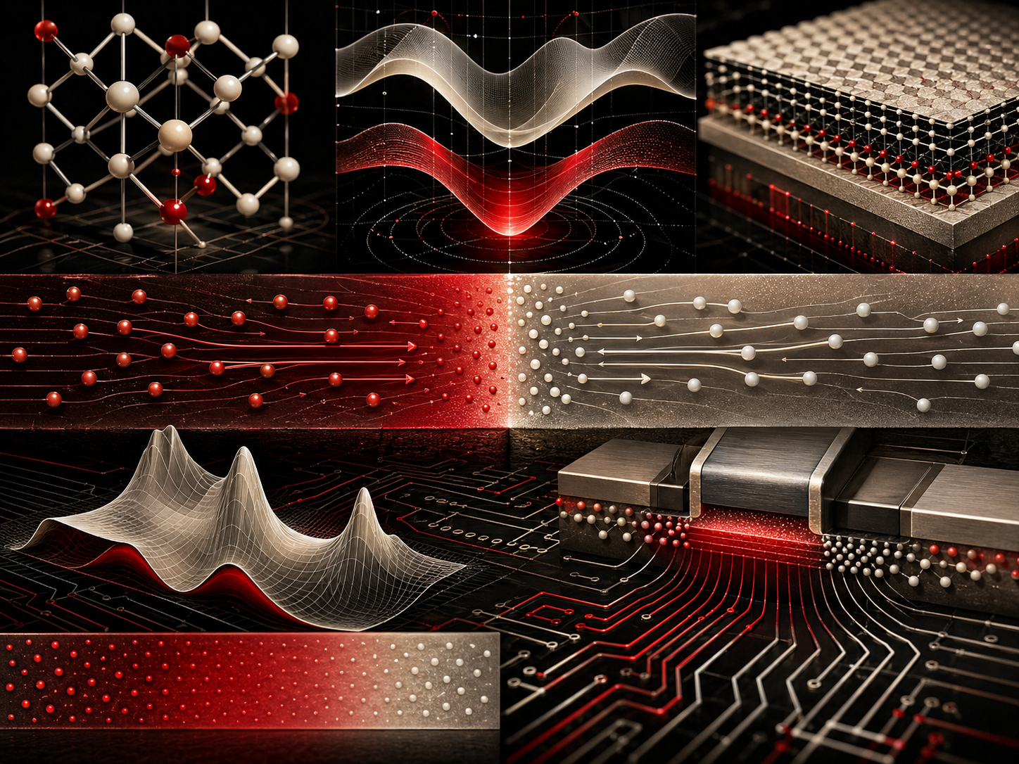
Semiconductor physics and electronic materials explain how quantum band structure, carrier statistics, doping, defects, interfaces, electric fields, and transport processes make modern electronics possible. A semiconductor is neither simply a conductor nor simply an insulator. Its electrical behavior depends on the energy gap between valence and conduction bands, the position of the Fermi level, the density of carriers, temperature, impurities, crystal structure, interfaces, and applied fields. By controlling these variables, physicists and engineers can build diodes, transistors, photodetectors, solar cells, light-emitting devices, sensors, integrated circuits, memory, power electronics, and quantum devices.
Semiconductor physics is one of the clearest examples of quantum mechanics becoming technological infrastructure. Electrons in crystals do not behave like isolated particles in free space. They occupy allowed energy bands shaped by periodic atomic potentials. Near band extrema, their motion can often be described using effective mass. Thermal excitation, doping, and electrostatic fields determine carrier populations. Drift, diffusion, recombination, and generation determine current flow. Interfaces and junctions shape device behavior. Materials quality, defects, strain, surfaces, oxides, and contacts determine whether theoretical performance can actually be realized.
This article examines Semiconductor Physics and Electronic Materials as part of the Physics knowledge series, connecting quantum band structure, crystal lattices, carrier statistics, intrinsic and extrinsic semiconductors, doping, mobility, conductivity, drift, diffusion, recombination, p–n junctions, depletion regions, diode current, metal–semiconductor contacts, MOS capacitors, MOSFET physics, defects, strain, interfaces, heterostructures, compound semiconductors, wide-bandgap materials, optoelectronics, semiconductor metrology, and computational modeling. Selected R and Python workflows appear in the article body, while the companion GitHub repository contains expanded computational resources for band diagrams, intrinsic carrier concentration, Fermi-level placement, conductivity, drift–diffusion, p–n junction electrostatics, diode curves, MOS capacitance, mobility models, uncertainty propagation, SQL metadata, C/C++/Fortran/Rust examples, and reproducible semiconductor-physics workflows.
Main Library
Publications
Article Map
Physics
Related Topic
Chemistry
Related Topic
Data Systems & Analytics
Related Topic
Astronomy
Why Semiconductor Physics Matters
Semiconductor physics matters because modern electronic civilization depends on the controlled behavior of electrons and holes in materials. Logic, memory, sensors, communications, power conversion, photovoltaics, imaging, computation, radio-frequency systems, quantum devices, and embedded electronics all depend on semiconductor materials whose carrier populations and transport properties can be engineered.
The central achievement of semiconductor technology is control. By introducing dopants, growing oxides, patterning gates, forming junctions, depositing contacts, engineering strain, selecting materials, and controlling interfaces, one can build structures whose electrical behavior is not found in the bulk material alone. A transistor is not simply a piece of silicon. It is an engineered electrostatic, quantum, and materials system.
Semiconductors also matter because they connect physics across scales. Quantum band structure determines allowed electronic states. Atomic impurities alter carrier density. Defects influence recombination and mobility. Interfaces control barriers and traps. Device geometry shapes electric fields. Circuits use many devices to process signals. Manufacturing variation affects system reliability. Semiconductor physics therefore links condensed matter, electromagnetism, thermodynamics, statistical mechanics, quantum mechanics, materials science, computational modeling, and measurement science.
For the Physics knowledge series, semiconductor physics is a crucial bridge between Quantum Mechanics and the Limits of Classical Intuition, Condensed Matter and the Physics of Materials, Electromagnetism and the Unification of Fields, Computational Physics and Scientific Simulation, and modern technology. It shows how microscopic states become macroscopic device function.
Semiconductors Between Metals and Insulators
Materials can be broadly classified by how easily they support electrical conduction. Metals have partially filled bands or overlapping bands, allowing many electrons to move under an applied field. Insulators have large band gaps, making thermal excitation of carriers difficult at ordinary temperatures. Semiconductors occupy an intermediate regime: their band gaps are large enough to suppress metallic conduction but small enough that carrier concentrations can be controlled by temperature, light, impurities, and electric fields.
This intermediate behavior is what makes semiconductors useful. A semiconductor can be made more conductive by adding donor or acceptor dopants. It can be depleted of carriers by electrostatic fields. It can absorb photons and generate electron–hole pairs. It can form junctions where internal electric fields separate charge. It can support field-effect control, allowing a gate voltage to modulate current.
The basic distinction can be described using the valence band, conduction band, and band gap:
E_g = E_c – E_v
\]
Interpretation: The band gap is the energy separation between the conduction-band edge and valence-band edge.
where \(E_g\) is the band gap, \(E_c\) is the conduction-band edge, and \(E_v\) is the valence-band edge. Electrons in the conduction band and holes in the valence band act as mobile carriers.
Semiconductor physics begins with the fact that conductivity is not fixed. It is a controllable material property shaped by carrier concentration and mobility.
Crystal Lattices and Periodic Potentials
Many important semiconductors are crystalline solids. Silicon, germanium, gallium arsenide, gallium nitride, silicon carbide, indium phosphide, and many other electronic materials have atomic arrangements that create periodic potentials for electrons. In a crystal, the potential energy experienced by an electron has the periodicity of the lattice:
V(\mathbf{r}+\mathbf{R}) = V(\mathbf{r})
\]
Interpretation: A crystal potential repeats under lattice translations.
where \(\mathbf{R}\) is a lattice translation vector. This periodicity changes the allowed electron states. Instead of free-particle energies alone, electrons occupy Bloch states:
\psi_{n\mathbf{k}}(\mathbf{r})
=
u_{n\mathbf{k}}(\mathbf{r})e^{i\mathbf{k}\cdot\mathbf{r}}
\]
Interpretation: Bloch states combine a plane-wave factor with a lattice-periodic function.
where \(u_{n\mathbf{k}}\) has the periodicity of the crystal lattice, \(n\) is a band index, and \(\mathbf{k}\) is a crystal wave vector.
The periodic lattice creates allowed bands and forbidden gaps. This is the foundation of electronic materials. A semiconductor is not defined only by which atoms it contains, but by how the crystal potential organizes electronic states.
Crystalline quality matters. Defects, dislocations, grain boundaries, impurities, strain, and interface disorder can all disturb the ideal periodic potential. These disturbances can create localized states, scatter carriers, shift band edges, trap charge, or accelerate recombination.
Energy Bands and Band Gaps
Energy bands describe the allowed electron energies in a crystal. The valence band is typically the highest occupied band at low temperature. The conduction band is a higher-energy band that can support mobile electrons. The band gap separates them:
E_g = E_c – E_v
\]
Interpretation: The band gap determines the minimum energy needed to promote an electron from valence to conduction states.
Band gaps may be direct or indirect. In a direct band-gap semiconductor, the conduction-band minimum and valence-band maximum occur at the same crystal momentum. Optical transitions can occur efficiently because photon momentum is small. Direct band-gap materials such as gallium arsenide and gallium nitride are important for light emission and optoelectronics.
In an indirect band-gap semiconductor, the conduction-band minimum and valence-band maximum occur at different crystal momenta. Optical transitions generally require phonon participation to conserve momentum. Silicon is an indirect band-gap semiconductor, which helps explain why it is excellent for electronics but inefficient as a light emitter.
The band gap influences carrier concentration, optical absorption, device voltage, thermal leakage, radiation response, and high-temperature performance. Wide-bandgap semiconductors such as silicon carbide and gallium nitride can support high electric fields, high temperatures, and power electronics applications. Narrower-gap materials may be useful for infrared detection or high-speed electronics.
Effective Mass, Density of States, and Carrier Motion
Electrons in a crystal respond to forces as if they have an effective mass determined by band curvature. Near a band extremum, energy can often be approximated by a parabolic relation:
E(\mathbf{k})
\approx
E_c
+
\frac{\hbar^2 k^2}{2m_n^*}
\]
Interpretation: Near the conduction-band edge, electron motion can often be approximated using an effective mass.
for electrons near the conduction-band edge, or:
E(\mathbf{k})
\approx
E_v
–
\frac{\hbar^2 k^2}{2m_p^*}
\]
Interpretation: Near the valence-band edge, hole behavior can be described using a positive effective mass.
for holes near the valence-band edge. The effective mass is related to band curvature:
\frac{1}{m^*}
=
\frac{1}{\hbar^2}
\frac{d^2E}{dk^2}
\]
Interpretation: Effective mass is determined by the curvature of the energy band.
A strongly curved band corresponds to a small effective mass. A flatter band corresponds to a larger effective mass. Effective mass affects mobility, density of states, carrier concentration, tunneling, and quantum confinement.
The density of states describes how many electronic states are available per unit energy. In a three-dimensional parabolic band, the density of states near a band edge scales with the square root of energy measured from that edge. Carrier concentration depends on both the density of available states and the probability that those states are occupied.
Effective mass is therefore more than a mathematical convenience. It is the bridge between quantum band structure and semiclassical transport.
Fermi–Dirac Statistics and the Fermi Level
Electrons are fermions, so their occupation of energy states follows Fermi–Dirac statistics:
f(E)
=
\frac{1}{1+\exp\left(\frac{E-E_F}{k_B T}\right)}
\]
Interpretation: The Fermi–Dirac function gives the probability that an electronic state is occupied.
where \(f(E)\) is the probability that a state of energy \(E\) is occupied, \(E_F\) is the Fermi level, \(k_B\) is Boltzmann’s constant, and \(T\) is absolute temperature.
The Fermi level is not simply the highest occupied energy in a semiconductor at ordinary temperature. It is the chemical potential for electrons and determines carrier populations. In intrinsic semiconductors, the Fermi level lies near the middle of the band gap, adjusted by effective density-of-states asymmetry. In n-type material, donor doping moves the Fermi level closer to the conduction band. In p-type material, acceptor doping moves it closer to the valence band.
In the nondegenerate approximation, carrier concentrations are often written as:
n
=
N_c
\exp\left(
-\frac{E_c-E_F}{k_B T}
\right)
\]
Interpretation: Electron concentration depends exponentially on the distance between the conduction-band edge and Fermi level.
p
=
N_v
\exp\left(
-\frac{E_F-E_v}{k_B T}
\right)
\]
Interpretation: Hole concentration depends exponentially on the distance between the Fermi level and valence-band edge.
where \(N_c\) and \(N_v\) are effective densities of states for the conduction and valence bands. These equations show that small shifts in Fermi level can produce exponential changes in carrier concentration.
Intrinsic Semiconductors
An intrinsic semiconductor is an ideally pure semiconductor whose carriers arise from thermal excitation across the band gap. At thermal equilibrium, electrons in the conduction band and holes in the valence band are generated in pairs, so:
n = p = n_i
\]
Interpretation: In an intrinsic semiconductor, electron and hole concentrations are equal.
where \(n_i\) is the intrinsic carrier concentration. In the nondegenerate approximation:
n_i
=
\sqrt{N_cN_v}
\exp\left(
-\frac{E_g}{2k_B T}
\right)
\]
Interpretation: Intrinsic carrier concentration depends exponentially on band gap and temperature.
This equation shows why band gap and temperature are so important. Carrier concentration depends exponentially on \(-E_g/(2k_B T)\). A larger band gap produces much lower intrinsic carrier concentration at the same temperature. Higher temperature increases intrinsic carriers dramatically.
The mass-action relation is:
np = n_i^2
\]
Interpretation: At equilibrium, electron and hole concentrations are linked by the intrinsic carrier concentration.
for a semiconductor in thermal equilibrium under nondegenerate conditions. This relation remains useful even in doped semiconductors when equilibrium assumptions apply.
Intrinsic carrier concentration is central to leakage current, temperature sensitivity, device isolation, and material selection. Silicon’s moderate band gap is one reason it became such a powerful electronic material, but high-temperature or high-power applications often require wider-bandgap materials.
Extrinsic Semiconductors and Doping
Extrinsic semiconductors are intentionally doped with impurity atoms that donate or accept carriers. Donor atoms introduce energy levels near the conduction band and can supply electrons. Acceptor atoms introduce levels near the valence band and can supply holes.
In an n-type semiconductor, electrons are majority carriers:
n \approx N_D
\]
Interpretation: In fully ionized, uncompensated n-type material, electron concentration is approximately donor concentration.
when donors are fully ionized and compensation is negligible. In a p-type semiconductor, holes are majority carriers:
p \approx N_A
\]
Interpretation: In fully ionized, uncompensated p-type material, hole concentration is approximately acceptor concentration.
under analogous conditions. The minority carrier concentration follows from the mass-action relation:
p \approx \frac{n_i^2}{N_D}
\]
Interpretation: In n-type material, minority hole concentration decreases as donor concentration increases.
for n-type material, and:
n \approx \frac{n_i^2}{N_A}
\]
Interpretation: In p-type material, minority electron concentration decreases as acceptor concentration increases.
for p-type material.
Doping is one of the core control mechanisms of semiconductor technology. It changes conductivity, junction behavior, depletion width, threshold voltage, contact resistance, breakdown behavior, and carrier lifetime. But doping also introduces ionized impurity scattering, possible compensation, diffusion, activation limits, and process variability. In modern devices, precise dopant placement and concentration control can be as important as the nominal material itself.
Mobility, Conductivity, and Transport
Carrier mobility describes how quickly carriers drift in response to an electric field. For electrons:
v_n = \mu_n E
\]
Interpretation: Electron drift velocity is proportional to electric field in the low-field mobility regime.
and for holes:
v_p = \mu_p E
\]
Interpretation: Hole drift velocity is proportional to electric field in the low-field mobility regime.
where \(v\) is drift velocity, \(\mu\) is mobility, and \(E\) is electric field. At high fields, velocity saturation and other nonlinear transport effects can occur, so this simple linear relation has limits.
The electrical conductivity of a semiconductor is:
\sigma
=
q(n\mu_n+p\mu_p)
\]
Interpretation: Conductivity depends on carrier charge, concentrations, and mobilities.
where \(q\) is the elementary charge, \(n\) is electron concentration, \(p\) is hole concentration, and \(\mu_n,\mu_p\) are electron and hole mobilities. Resistivity is:
\rho = \frac{1}{\sigma}
\]
Interpretation: Resistivity is the inverse of conductivity.
Mobility depends on scattering. Lattice vibrations, ionized impurities, defects, alloy disorder, interface roughness, phonons, and carrier-carrier interactions can all reduce mobility. Temperature and doping therefore affect conductivity in competing ways: increasing temperature can increase intrinsic carrier concentration while also increasing phonon scattering.
Transport connects material quality to device performance. Two materials with similar band gaps may behave very differently if one has higher mobility, fewer defects, better interfaces, or stronger scattering suppression.
Drift, Diffusion, Generation, and Recombination
Semiconductor current has both drift and diffusion components. Drift current arises from electric fields. Diffusion current arises from carrier concentration gradients.
Electron current density can be written as:
J_n
=
q n\mu_n E
+
qD_n\nabla n
\]
Interpretation: Electron current combines drift from electric fields and diffusion from concentration gradients.
Hole current density can be written as:
J_p
=
q p\mu_p E
–
qD_p\nabla p
\]
Interpretation: Hole current combines drift and diffusion with sign conventions appropriate for positive carriers.
where \(D_n\) and \(D_p\) are diffusion coefficients. The Einstein relation links diffusion and mobility under thermal equilibrium conditions:
D = \mu \frac{k_B T}{q}
\]
Interpretation: Diffusion and mobility are linked by thermal energy under equilibrium assumptions.
Generation creates electron–hole pairs. Recombination annihilates them. Recombination mechanisms include radiative recombination, Shockley–Read–Hall recombination through defects, and Auger recombination. Carrier lifetime strongly affects diodes, solar cells, LEDs, photodetectors, and power devices.
The continuity equation expresses charge conservation. For electrons:
\frac{\partial n}{\partial t}
=
\frac{1}{q}\nabla\cdot J_n
+
G_n
–
R_n
\]
Interpretation: Electron concentration changes through current divergence, generation, and recombination.
where \(G_n\) is generation and \(R_n\) is recombination. Drift–diffusion theory, coupled with Poisson’s equation, is one of the central computational frameworks for semiconductor device simulation.
P–N Junctions and Depletion Regions
A p–n junction is formed when p-type and n-type semiconductor regions meet. Electrons diffuse from the n side toward the p side, and holes diffuse from the p side toward the n side. This diffusion leaves behind ionized donors and acceptors, creating a depletion region with an internal electric field.
The built-in potential for an ideal abrupt junction is:
V_{bi}
=
\frac{k_B T}{q}
\ln\left(
\frac{N_A N_D}{n_i^2}
\right)
\]
Interpretation: Built-in potential depends logarithmically on doping concentrations and intrinsic carrier concentration.
where \(N_A\) and \(N_D\) are acceptor and donor concentrations. The depletion width under an applied voltage \(V\) can be approximated as:
W
=
\sqrt{
\frac{2\epsilon_s}{q}
\left(
\frac{N_A+N_D}{N_A N_D}
\right)
(V_{bi}-V)
}
\]
Interpretation: Depletion width grows with permittivity and barrier potential and shrinks with heavier doping.
where \(\epsilon_s\) is semiconductor permittivity. Reverse bias increases the depletion width; forward bias decreases the barrier and allows current to flow more easily.
The p–n junction is foundational because it creates rectification, photovoltaic separation, light emission, depletion capacitance, breakdown behavior, and carrier injection. It is the basic building block behind many semiconductor devices.
Diode Current and Rectification
The ideal diode equation is:
I
=
I_s
\left[
\exp\left(
\frac{qV}{nk_B T}
\right)
–
1
\right]
\]
Interpretation: Ideal diode current rises exponentially under forward bias and approaches saturation under reverse bias.
where \(I_s\) is saturation current, \(V\) is applied voltage, and \(n\) is the ideality factor. When forward biased, current increases exponentially. When reverse biased, current is small until breakdown mechanisms become significant.
Rectification arises because the junction responds asymmetrically to applied voltage. Forward bias lowers the barrier and supports carrier injection. Reverse bias widens the depletion region and suppresses ordinary current flow, though leakage and breakdown remain important in real devices.
Real diodes deviate from the ideal equation. Series resistance matters at high current. Recombination in the depletion region changes ideality factor. Leakage affects reverse bias. High-level injection changes carrier distributions. Breakdown can occur through avalanche or tunneling. Temperature strongly affects saturation current because carrier concentrations and recombination rates are temperature-dependent.
The diode is therefore both a simple device and a rich physical system. It combines electrostatics, carrier statistics, transport, recombination, and material quality.
Metal–Semiconductor Contacts
Metal–semiconductor contacts determine how current enters and leaves a semiconductor device. A contact may behave approximately ohmically, allowing current to pass with low resistance, or it may form a Schottky barrier, producing rectifying behavior.
The Schottky barrier height depends on work function, electron affinity, interface states, Fermi-level pinning, surface chemistry, and processing conditions. A simplified n-type barrier relation is:
\Phi_{Bn}
\approx
\Phi_M – \chi
\]
Interpretation: A simplified Schottky barrier estimate subtracts semiconductor electron affinity from metal work function.
where \(\Phi_M\) is metal work function and \(\chi\) is semiconductor electron affinity. Real interfaces often deviate from this simple rule because interface states and chemical bonding can pin the Fermi level.
Contacts are crucial because even a well-designed semiconductor channel can fail if contact resistance is too high. In scaled devices, contact resistance can dominate performance. In power devices, contacts must handle high current and temperature. In optoelectronics, contacts must balance conductivity, transparency, and recombination control.
Semiconductor interfaces are never passive details. They are active parts of the device physics.
MOS Capacitors and Field-Effect Control
The metal–oxide–semiconductor capacitor is one of the most important structures in electronics. It consists of a conducting gate, an insulating oxide, and a semiconductor substrate. By applying a gate voltage, one can alter the charge distribution near the semiconductor surface.
Depending on gate voltage, a MOS capacitor can be in accumulation, depletion, or inversion. In a p-type substrate, a positive gate voltage can repel holes and eventually attract electrons to form an inversion layer. This field-effect control allows a gate voltage to modulate conductivity without injecting current through the oxide in the ideal case.
The oxide capacitance per unit area is:
C_{ox}
=
\frac{\epsilon_{ox}}{t_{ox}}
\]
Interpretation: Oxide capacitance per unit area increases with permittivity and decreases with oxide thickness.
where \(\epsilon_{ox}\) is oxide permittivity and \(t_{ox}\) is oxide thickness. Thinner oxides increase gate control, but leakage, reliability, tunneling, dielectric breakdown, and interface quality become critical.
MOS physics brings together electrostatics, quantum confinement, interface traps, oxide charge, threshold voltage, capacitance, inversion layers, and materials engineering. It is the foundation of the MOSFET.
MOSFETs and Transistor Physics
The metal–oxide–semiconductor field-effect transistor, or MOSFET, controls current through a semiconductor channel using an electric field from a gate. In an n-channel MOSFET on a p-type substrate, a sufficiently positive gate voltage creates an inversion layer connecting source and drain. Current then flows when a drain voltage is applied.
A simplified long-channel MOSFET current in the linear regime is:
I_D
\approx
\mu_n C_{ox}\frac{W}{L}
\left[
(V_{GS}-V_T)V_{DS}
–
\frac{V_{DS}^2}{2}
\right]
\]
Interpretation: In the long-channel linear regime, drain current depends on mobility, gate capacitance, geometry, and applied voltages.
where \(W\) is channel width, \(L\) is channel length, \(V_{GS}\) is gate-source voltage, \(V_{DS}\) is drain-source voltage, and \(V_T\) is threshold voltage. In saturation, an idealized expression is:
I_D
\approx
\frac{1}{2}
\mu_n C_{ox}\frac{W}{L}
(V_{GS}-V_T)^2
\]
Interpretation: In the idealized saturation regime, current scales quadratically with gate overdrive.
These equations are simplified. Real MOSFETs exhibit velocity saturation, mobility degradation, short-channel effects, drain-induced barrier lowering, quantum confinement, leakage, contact resistance, variability, self-heating, and reliability effects.
Transistor scaling has required increasingly sophisticated materials and structures: high-\(k\) dielectrics, metal gates, strained channels, silicon-on-insulator technologies, FinFETs, gate-all-around devices, compound semiconductors, and new integration approaches. Semiconductor physics remains central because device architecture changes, but carrier statistics, fields, transport, and materials limits remain.
Electronic Materials, Defects, and Interfaces
Electronic materials are judged not only by ideal band structure but also by real material quality. Defects can introduce trap states in the band gap, scatter carriers, reduce mobility, promote recombination, shift thresholds, create leakage paths, and degrade reliability.
Important defect types include vacancies, interstitials, substitutional impurities, dislocations, grain boundaries, interface traps, oxide charges, and surface states. In some contexts, defects are harmful. In others, they can be engineered for functionality, as in dopants, color centers, or quantum defects. The difference lies in control.
Interfaces are especially important. A semiconductor device may depend on the interface between silicon and silicon dioxide, a metal and a semiconductor, a high-\(k\) dielectric and a channel, a heterojunction between two semiconductors, or a contact layer and active material. Interface states can trap charge, scatter carriers, pin the Fermi level, or modify band alignment.
Electronic materials therefore require physics, chemistry, crystallography, thermodynamics, surface science, fabrication control, and metrology. The ideal equations of semiconductor physics must be interpreted through the imperfections of actual materials.
Heterostructures, Compound Semiconductors, and Wide-Bandgap Materials
A heterostructure joins materials with different band gaps, electron affinities, lattice constants, or dielectric properties. Band offsets at the interface can confine carriers, separate electrons and holes, form quantum wells, create high-mobility channels, or engineer optical transitions.
Compound semiconductors such as gallium arsenide, indium phosphide, gallium nitride, and related alloys are important because their band gaps, mobilities, optical properties, and lattice constants can be engineered. Direct band-gap compound semiconductors are central to LEDs, lasers, photodetectors, and high-frequency devices.
Wide-bandgap semiconductors such as silicon carbide and gallium nitride are important for high-power, high-voltage, high-temperature, and high-frequency applications. Their large band gaps can reduce intrinsic carrier concentration and leakage at elevated temperatures. Their high breakdown fields can support compact power devices.
Heterostructures show that electronic materials are not only selected; they are designed. By combining materials, one can create energy landscapes that do not exist in a single homogeneous crystal.
Optoelectronic and Photovoltaic Materials
Semiconductors interact strongly with light when photon energy is comparable to or greater than the band gap. Absorption can generate electron–hole pairs:
h\nu \geq E_g
\]
Interpretation: Photons with energy at or above the band gap can generate electron–hole pairs.
This principle underlies photodetectors and solar cells. In a photovoltaic device, absorbed light generates carriers, and internal electric fields or selective contacts help separate them before recombination. The p–n junction is one way to create this separation.
Light-emitting devices work in the reverse direction. Electrons and holes recombine and emit photons. Efficient light emission generally requires materials and structures that support radiative recombination. Direct band-gap semiconductors are usually better light emitters than indirect band-gap materials.
Optoelectronic materials require attention to band gap, absorption coefficient, carrier lifetime, diffusion length, mobility, radiative efficiency, defects, surfaces, contacts, thermal properties, and optical confinement. A photovoltaic material must absorb light and collect carriers efficiently. A light-emitting material must inject carriers and emit photons efficiently. A detector must convert photons into measurable electrical signals with low noise.
Semiconductor Metrology and Reproducibility
Semiconductor metrology is the measurement science that makes semiconductor materials and devices trustworthy, manufacturable, and comparable. Important measurements include film thickness, composition, carrier concentration, mobility, resistivity, sheet resistance, interface trap density, strain, critical dimension, defect density, optical response, capacitance, current–voltage behavior, and reliability metrics.
Measurement becomes more difficult as devices become smaller, multilayered, three-dimensional, heterogeneous, and more sensitive to nanoscale variation. A measurement must be accurate, precise, traceable, and fit for its intended purpose. It must also be connected to a physical model: measuring a current-voltage curve is not the same as understanding which transport mechanism dominates.
Reproducibility requires documenting units, temperature, sample geometry, material stack, dopant concentration, bias conditions, illumination, contact method, instrument settings, calibration, uncertainty, and data-processing steps. Semiconductor data without context can be misleading because measured properties depend strongly on conditions.
Computational workflows should therefore include metadata. A diode simulation should record temperature, saturation current, ideality factor, area, voltage range, and assumptions. A conductivity calculation should record mobility model, carrier concentration, units, and doping regime. A band-diagram calculation should record material parameters, boundary conditions, and reference energy conventions.
Measurement, Units, and SI Interpretation
Semiconductor physics uses both SI units and discipline-specific units. Energies are often expressed in electronvolts:
1\ \mathrm{eV}
=
q \times 1\ \mathrm{V}
\]
Interpretation: One electronvolt is the energy gained by one elementary charge across one volt.
Carrier concentration is often expressed in \(\mathrm{cm^{-3}}\), though SI base units use \(\mathrm{m^{-3}}\). Mobility is often expressed in \(\mathrm{cm^2\,V^{-1}\,s^{-1}}\), while SI uses \(\mathrm{m^2\,V^{-1}\,s^{-1}}\). Electric field may be expressed in \(\mathrm{V\,cm^{-1}}\) or \(\mathrm{V\,m^{-1}}\). Current density may be expressed in \(\mathrm{A\,cm^{-2}}\) or \(\mathrm{A\,m^{-2}}\).
The thermal voltage is:
V_T
=
\frac{k_B T}{q}
\]
Interpretation: Thermal voltage converts thermal energy into an equivalent voltage scale.
At room temperature near \(300\ \mathrm{K}\), this is approximately:
V_T \approx 25.9\ \mathrm{mV}
\]
Interpretation: Room-temperature thermal voltage sets a key exponential scale in semiconductor equations.
Conductivity has SI units:
\mathrm{S\,m^{-1}}
\]
Interpretation: Conductivity measures electrical conductance per unit length scale.
and resistivity has units:
\Omega\,\mathrm{m}
\]
Interpretation: Resistivity measures resistance normalized by material geometry.
Unit consistency is essential because semiconductor calculations often combine electronvolts, volts, kelvin, centimeters, meters, coulombs, joules, and carrier densities. A common error is mixing \(\mathrm{cm^{-3}}\) and \(\mathrm{m^{-3}}\) without conversion. Reproducible semiconductor computation should make unit conversions explicit.
Mathematical Lens
A mathematics-first view of semiconductor physics begins with band structure and carrier statistics. The band gap is:
E_g = E_c – E_v
\]
Interpretation: Band gap separates conduction and valence band edges.
The Fermi–Dirac occupation probability is:
f(E)
=
\frac{1}{1+\exp\left(\frac{E-E_F}{k_B T}\right)}
\]
Interpretation: Fermi–Dirac statistics determine electronic occupation probabilities.
In the nondegenerate approximation, electron and hole concentrations are:
n
=
N_c
\exp\left(
-\frac{E_c-E_F}{k_B T}
\right)
\]
Interpretation: Electron concentration is controlled by Fermi-level position relative to the conduction band.
p
=
N_v
\exp\left(
-\frac{E_F-E_v}{k_B T}
\right)
\]
Interpretation: Hole concentration is controlled by Fermi-level position relative to the valence band.
The intrinsic carrier concentration is:
n_i
=
\sqrt{N_cN_v}
\exp\left(
-\frac{E_g}{2k_B T}
\right)
\]
Interpretation: Intrinsic carrier concentration is exponentially sensitive to band gap and temperature.
Conductivity is:
\sigma
=
q(n\mu_n+p\mu_p)
\]
Interpretation: Conductivity combines electron and hole contributions.
Drift–diffusion current densities are:
J_n
=
q n\mu_n E
+
qD_n\nabla n
\]
Interpretation: Electron current combines drift and diffusion terms.
J_p
=
q p\mu_p E
–
qD_p\nabla p
\]
Interpretation: Hole current combines drift and diffusion terms with carrier sign convention.
Poisson’s equation relates electrostatic potential \(\phi\) to charge density:
\nabla\cdot(\epsilon\nabla\phi)
=
-\rho
\]
Interpretation: Poisson’s equation connects electrostatic potential to charge distribution.
The p–n junction built-in potential is:
V_{bi}
=
\frac{k_B T}{q}
\ln\left(
\frac{N_A N_D}{n_i^2}
\right)
\]
Interpretation: Built-in potential follows from equilibrium carrier statistics across a junction.
The ideal diode equation is:
I
=
I_s
\left[
\exp\left(
\frac{qV}{nk_B T}
\right)
–
1
\right]
\]
Interpretation: Diode current depends exponentially on applied voltage relative to thermal voltage.
This mathematical lens shows how semiconductor physics moves from quantum bands to statistical carrier populations, from carrier populations to transport, from transport to device equations, and from device equations to circuits and systems.
Variables, Units, and Physical Interpretation
Semiconductor physics depends on variables that connect quantum energy structure, carrier statistics, transport, electrostatics, and device behavior. The table below summarizes several central quantities.
| Symbol or Term | Meaning | Typical Unit | Physical Interpretation |
|---|---|---|---|
| \(E_g\) | Band gap | eV or J | Energy separation between conduction and valence band edges |
| \(E_c\) | Conduction-band edge | eV or J | Lowest relevant energy of conduction-band states |
| \(E_v\) | Valence-band edge | eV or J | Highest relevant energy of valence-band states |
| \(E_F\) | Fermi level | eV or J | Electron chemical potential controlling state occupation |
| \(n\) | Electron concentration | cm\(^{-3}\) or m\(^{-3}\) | Mobile electrons in the conduction band |
| \(p\) | Hole concentration | cm\(^{-3}\) or m\(^{-3}\) | Mobile holes in the valence band |
| \(n_i\) | Intrinsic carrier concentration | cm\(^{-3}\) or m\(^{-3}\) | Carrier concentration in an ideal intrinsic semiconductor |
| \(N_D,N_A\) | Donor and acceptor concentrations | cm\(^{-3}\) or m\(^{-3}\) | Doping concentrations controlling majority carriers |
| \(\mu_n,\mu_p\) | Electron and hole mobility | cm²/V/s or m²/V/s | Carrier drift response to electric field |
| \(\sigma\) | Conductivity | S/m | Ability of material to conduct electrical current |
| \(D_n,D_p\) | Diffusion coefficients | m²/s | Carrier spreading due to concentration gradients |
| \(V_{bi}\) | Built-in potential | V | Equilibrium potential across a p–n junction |
Note: Semiconductor variables connect quantum energy structure, carrier populations, transport, electrostatics, and device behavior. A useful semiconductor model must keep all of these levels connected.
Worked Example: Intrinsic Carrier Concentration
Consider an idealized silicon-like semiconductor at \(T=300\ \mathrm{K}\), with:
E_g = 1.12\ \mathrm{eV}
\]
Interpretation: The band gap sets the energy barrier for intrinsic carrier generation.
N_c = 2.8\times10^{19}\ \mathrm{cm^{-3}}
\]
Interpretation: \(N_c\) is the conduction-band effective density of states.
N_v = 1.04\times10^{19}\ \mathrm{cm^{-3}}
\]
Interpretation: \(N_v\) is the valence-band effective density of states.
The intrinsic carrier concentration is:
n_i
=
\sqrt{N_cN_v}
\exp\left(
-\frac{E_g}{2k_B T}
\right)
\]
Interpretation: Intrinsic carrier concentration combines density of states with exponential thermal activation.
Using \(k_B T \approx 0.02585\ \mathrm{eV}\) at \(300\ \mathrm{K}\):
\frac{E_g}{2k_B T}
=
\frac{1.12}{2(0.02585)}
\approx
21.66
\]
Interpretation: The exponential activation factor is large even for a moderate semiconductor band gap.
The effective density-of-states factor is:
\sqrt{N_cN_v}
=
\sqrt{
(2.8\times10^{19})(1.04\times10^{19})
}
\]
Interpretation: The density-of-states prefactor is the geometric mean of conduction and valence effective densities.
\sqrt{N_cN_v}
\approx
1.71\times10^{19}\ \mathrm{cm^{-3}}
\]
Interpretation: The prefactor is enormous compared with the final thermally activated carrier concentration.
Therefore:
n_i
\approx
(1.71\times10^{19})
e^{-21.66}
\]
Interpretation: The exponential factor strongly suppresses intrinsic carriers.
n_i
\approx
6.7\times10^{9}\ \mathrm{cm^{-3}}
\]
Interpretation: The intrinsic carrier concentration is many orders of magnitude below the density-of-states scale.
This is an order-of-magnitude educational calculation. More precise values depend on temperature-dependent band gap, effective masses, density-of-states parameters, material purity, and empirical corrections. The important point is the exponential sensitivity: a modest band gap produces a very small intrinsic carrier concentration compared with atomic density.
Computational Modeling
Computational modeling helps turn semiconductor physics into reproducible analysis. A carrier-concentration model can compute intrinsic and doped carrier populations. A conductivity model can combine mobility and carrier density. A p–n junction model can estimate built-in potential and depletion width. A diode model can compute current–voltage curves. A MOS model can estimate oxide capacitance, threshold behavior, and charge regimes. A drift–diffusion solver can couple Poisson’s equation to carrier transport. A metadata system can preserve material parameters, units, temperature, device geometry, and assumptions.
The selected examples below focus on conductivity sensitivity and diode current-voltage behavior because they are foundational, readable, and widely reusable. The GitHub repository extends the same logic into richer computational resources: R conductivity and doping sensitivity workflows, Python diode and p–n junction models, intrinsic carrier concentration calculations, Fermi-level placement, MOS capacitance, mobility models, uncertainty propagation, Julia semiconductor calculations, C++ transport sweeps, Fortran junction tables, SQL semiconductor-physics metadata, Rust command-line utilities, C examples, documentation, and reproducible sample data.
R Workflow: Conductivity Sensitivity to Doping and Mobility
R is useful for parameter sweeps, sensitivity tables, and reproducible semiconductor calculations. The following workflow estimates conductivity and resistivity for n-type semiconductor cases using majority-carrier electron conduction.
# Conductivity Sensitivity to Doping and Mobility
#
# This workflow estimates conductivity:
#
#   sigma = q n mu_n
#
# for n-type semiconductor cases where electron concentration is
# approximated by donor concentration.
#
# Unit conventions:
#   carrier concentration is given in cm^-3
#   mobility is given in cm^2 / V / s
#
# These are converted to SI:
#   cm^-3 -> m^-3
#   cm^2 / V / s -> m^2 / V / s

library(tibble)
library(dplyr)
library(tidyr)

elementary_charge_c <- 1.602176634e-19

parameter_grid <- crossing(
  donor_concentration_cm3 = c(1e14, 1e15, 1e16, 1e17, 1e18),
  electron_mobility_cm2_v_s = c(100, 500, 1000, 1400)
) %>%
  mutate(
    donor_concentration_m3 = donor_concentration_cm3 * 1e6,
    electron_mobility_m2_v_s = electron_mobility_cm2_v_s * 1e-4,
    conductivity_s_m =
      elementary_charge_c *
      donor_concentration_m3 *
      electron_mobility_m2_v_s,
    resistivity_ohm_m = 1 / conductivity_s_m,
    resistivity_ohm_cm = resistivity_ohm_m * 100
  )

conductivity_summary <- parameter_grid %>%
  group_by(donor_concentration_cm3) %>%
  summarise(
    min_resistivity_ohm_cm = min(resistivity_ohm_cm),
    max_resistivity_ohm_cm = max(resistivity_ohm_cm),
    mean_conductivity_s_m = mean(conductivity_s_m),
    .groups = "drop"
  )

print(parameter_grid)
print(conductivity_summary)
This workflow shows how doping and mobility jointly determine conductivity. Increasing carrier concentration generally increases conductivity, but mobility is not fixed in real materials; it can decrease as impurity scattering rises. A more advanced model would make mobility a function of doping, temperature, field, and material quality.
Python Workflow: Diode Current–Voltage Curve
Python is useful for numerical device modeling, unit conversion, curve generation, and reproducible scientific computing. The following workflow computes an ideal diode current-voltage curve and records thermal voltage, saturation current, ideality factor, and current density.
"""
Diode Current-Voltage Curve

This workflow computes the ideal diode equation:

    I = I_s [ exp(q V / (n k_B T)) - 1 ]

where:
    I   = diode current, A
    I_s = saturation current, A
    q   = elementary charge, C
    V   = applied voltage, V
    n   = ideality factor
    k_B = Boltzmann constant, J/K
    T   = temperature, K

The model is intentionally idealized. Real diodes may require series
resistance, recombination current, high-level injection, breakdown,
temperature-dependent saturation current, and geometry-specific modeling.
"""

import numpy as np
import pandas as pd

ELEMENTARY_CHARGE_C = 1.602176634e-19
BOLTZMANN_CONSTANT_J_K = 1.380649e-23

TEMPERATURE_K = 300.0
IDEALITY_FACTOR = 1.0
SATURATION_CURRENT_A = 1.0e-12
DIODE_AREA_CM2 = 1.0e-4

def diode_current_a(voltage_v: np.ndarray) -> np.ndarray:
    """
    Compute ideal diode current for an array of voltages.
    """
    thermal_voltage_v = BOLTZMANN_CONSTANT_J_K * TEMPERATURE_K / ELEMENTARY_CHARGE_C

    exponent = voltage_v / (IDEALITY_FACTOR * thermal_voltage_v)

    # Clip exponent to avoid numerical overflow in exploratory calculations.
    exponent = np.clip(exponent, -100.0, 100.0)

    return SATURATION_CURRENT_A * (np.exp(exponent) - 1.0)

def main() -> None:
    """
    Generate an ideal diode current-voltage table.
    """
    voltage_v = np.linspace(-0.5, 0.8, 132)
    current_a = diode_current_a(voltage_v)

    thermal_voltage_v = BOLTZMANN_CONSTANT_J_K * TEMPERATURE_K / ELEMENTARY_CHARGE_C

    output = pd.DataFrame(
        {
            "voltage_v": voltage_v,
            "current_a": current_a,
            "current_density_a_cm2": current_a / DIODE_AREA_CM2,
            "temperature_k": TEMPERATURE_K,
            "thermal_voltage_v": thermal_voltage_v,
            "ideality_factor": IDEALITY_FACTOR,
            "saturation_current_a": SATURATION_CURRENT_A,
        }
    )

    selected = output[
        output["voltage_v"].round(2).isin([-0.5, -0.2, 0.0, 0.2, 0.4, 0.6, 0.8])
    ]

    print("Selected ideal diode I-V values:")
    print(selected.round(8).to_string(index=False))

    print("\nModel settings:")
    print(
        pd.DataFrame(
            [
                {
                    "temperature_k": TEMPERATURE_K,
                    "thermal_voltage_v": thermal_voltage_v,
                    "ideality_factor": IDEALITY_FACTOR,
                    "saturation_current_a": SATURATION_CURRENT_A,
                    "diode_area_cm2": DIODE_AREA_CM2,
                }
            ]
        ).round(10).to_string(index=False)
    )

if __name__ == "__main__":
    main()
This workflow shows the exponential character of ideal diode current. It also shows why numerical care is needed: exponentials can overflow, real devices depart from ideality, and measured curves require careful interpretation of area, temperature, series resistance, leakage, and breakdown behavior.
GitHub Repository
The article body includes only selected computational examples so the conceptual and mathematical argument remains readable. The full repository contains expanded computational resources: R conductivity and doping sensitivity workflows, Python diode and p–n junction models, intrinsic carrier concentration calculations, Fermi-level placement, MOS capacitance, mobility models, uncertainty propagation, Julia semiconductor calculations, C++ transport sweeps, Fortran junction tables, SQL semiconductor-physics metadata, Rust command-line utilities, C examples, documentation, and reproducible sample data.
From Semiconductor Physics to Electronic Systems
Semiconductor physics shows how quantum materials become functional electronic systems. Band structure defines allowed states. Carrier statistics determine populations. Doping moves the Fermi level. Electric fields drive carriers. Diffusion responds to gradients. Recombination and generation control lifetimes. Junctions create internal fields. Interfaces determine barriers and traps. Device geometry converts materials into transistors, diodes, detectors, emitters, and power devices.
Within the Physics knowledge series, this article belongs after Condensed Matter and the Physics of Materials, Quantum Mechanics and the Limits of Classical Intuition, Electromagnetism and the Unification of Fields, and Computational Physics and Scientific Simulation. It shows how microscopic electronic structure becomes engineered function.
The next conceptual steps are natural. Atomic, Molecular, and Optical Physics connects electronic transitions to light–matter interaction. Quantum Information, Decoherence, and Measurement connects physical qubits to semiconductor and solid-state platforms. Data Systems and Analytics provides the reproducible infrastructure needed for device data, metrology, and simulation outputs.
Related Articles
- What Is Physics?
- Measurement, Mathematics, and the Structure of Physical Inquiry
- Mathematical Methods in Physics
- Quantum Mechanics and the Limits of Classical Intuition
- Condensed Matter and the Physics of Materials
- Continuum Physics and Material Behavior
- Electromagnetism and the Unification of Fields
- Light, Waves, and the Physics of Radiation
- Atomic, Molecular, and Optical Physics
- Quantum Information, Decoherence, and Measurement
- Computational Physics and Scientific Simulation
- Data Systems and Analytics
Further Reading
- Ashcroft, N.W. and Mermin, N.D. (1976) Solid State Physics. New York: Holt, Rinehart and Winston. Publisher information available at: https://www.cengage.com/c/solid-state-physics-1e-ashcroft/ (Accessed: 25 April 2026).
- del Alamo, J.A. (2007) Integrated Microelectronic Devices. MIT OpenCourseWare. Available at: https://ocw.mit.edu/courses/6-720j-integrated-microelectronic-devices-spring-2007/ (Accessed: 25 April 2026).
- Kittel, C. (2005) Introduction to Solid State Physics, 8th edn. Hoboken: Wiley. Available at: https://www.wiley.com/en-us/Introduction+to+Solid+State+Physics%2C+8th+Edition-p-9780471415268 (Accessed: 25 April 2026).
- MIT OpenCourseWare (2003) Physics for Solid-State Applications. Available at: https://ocw.mit.edu/courses/6-730-physics-for-solid-state-applications-spring-2003/ (Accessed: 25 April 2026).
- MIT OpenCourseWare (2009) Microelectronic Devices and Circuits: Lecture Notes. Available at: https://ocw.mit.edu/courses/6-012-microelectronic-devices-and-circuits-fall-2009/pages/lecture-notes/ (Accessed: 25 April 2026).
- MIT OpenCourseWare (2012) Nano-to-Macro Transport Processes: PN Junction, Diode and Photovoltaic Cells. Available at: https://ocw.mit.edu/courses/2-57-nano-to-macro-transport-processes-spring-2012/resources/lecture-22-pn-junction-diode-and-photovoltaic-cells/ (Accessed: 25 April 2026).
- NIST (2024) CHIPS Metrology Program. Available at: https://www.nist.gov/chips/research-development-programs/metrology-program (Accessed: 25 April 2026).
- NIST (2025) Semiconductors. Available at: https://www.nist.gov/semiconductors (Accessed: 25 April 2026).
- NIST (2026) CODATA Internationally Recommended Values of the Fundamental Physical Constants. Available at: https://physics.nist.gov/cuu/Constants/ (Accessed: 25 April 2026).
- Pierret, R.F. (1996) Semiconductor Device Fundamentals. Boston: Addison-Wesley. Publisher information available at: https://www.pearson.com/en-us/subject-catalog/p/semiconductor-device-fundamentals/P200000003278 (Accessed: 25 April 2026).
- Sze, S.M. and Ng, K.K. (2006) Physics of Semiconductor Devices, 3rd edn. Hoboken: Wiley. Available at: https://www.wiley.com/en-us/Physics+of+Semiconductor+Devices%2C+3rd+Edition-p-9780471143239 (Accessed: 25 April 2026).
- Yu, P.Y. and Cardona, M. (2010) Fundamentals of Semiconductors: Physics and Materials Properties, 4th edn. Berlin: Springer. Available at: https://link.springer.com/book/10.1007/978-3-642-00710-1 (Accessed: 25 April 2026).
References
- del Alamo, J.A. (2007) Integrated Microelectronic Devices. MIT OpenCourseWare. Available at: https://ocw.mit.edu/courses/6-720j-integrated-microelectronic-devices-spring-2007/ (Accessed: 25 April 2026).
- MIT OpenCourseWare (2003) Physics for Solid-State Applications. Available at: https://ocw.mit.edu/courses/6-730-physics-for-solid-state-applications-spring-2003/ (Accessed: 25 April 2026).
- MIT OpenCourseWare (2009) Microelectronic Devices and Circuits: Lecture Notes. Available at: https://ocw.mit.edu/courses/6-012-microelectronic-devices-and-circuits-fall-2009/pages/lecture-notes/ (Accessed: 25 April 2026).
- NIST (2024) CHIPS Metrology Program. Available at: https://www.nist.gov/chips/research-development-programs/metrology-program (Accessed: 25 April 2026).
- NIST (2025) Semiconductors. Available at: https://www.nist.gov/semiconductors (Accessed: 25 April 2026).
- NIST (2026) CODATA Internationally Recommended Values of the Fundamental Physical Constants. Available at: https://physics.nist.gov/cuu/Constants/ (Accessed: 25 April 2026).
- Sze, S.M. and Ng, K.K. (2006) Physics of Semiconductor Devices, 3rd edn. Hoboken: Wiley. Available at: https://www.wiley.com/en-us/Physics+of+Semiconductor+Devices%2C+3rd+Edition-p-9780471143239 (Accessed: 25 April 2026).